
Nanofabrication Engineering Intern Resume Builder
Nanofabrication Engineering Intern resumes made
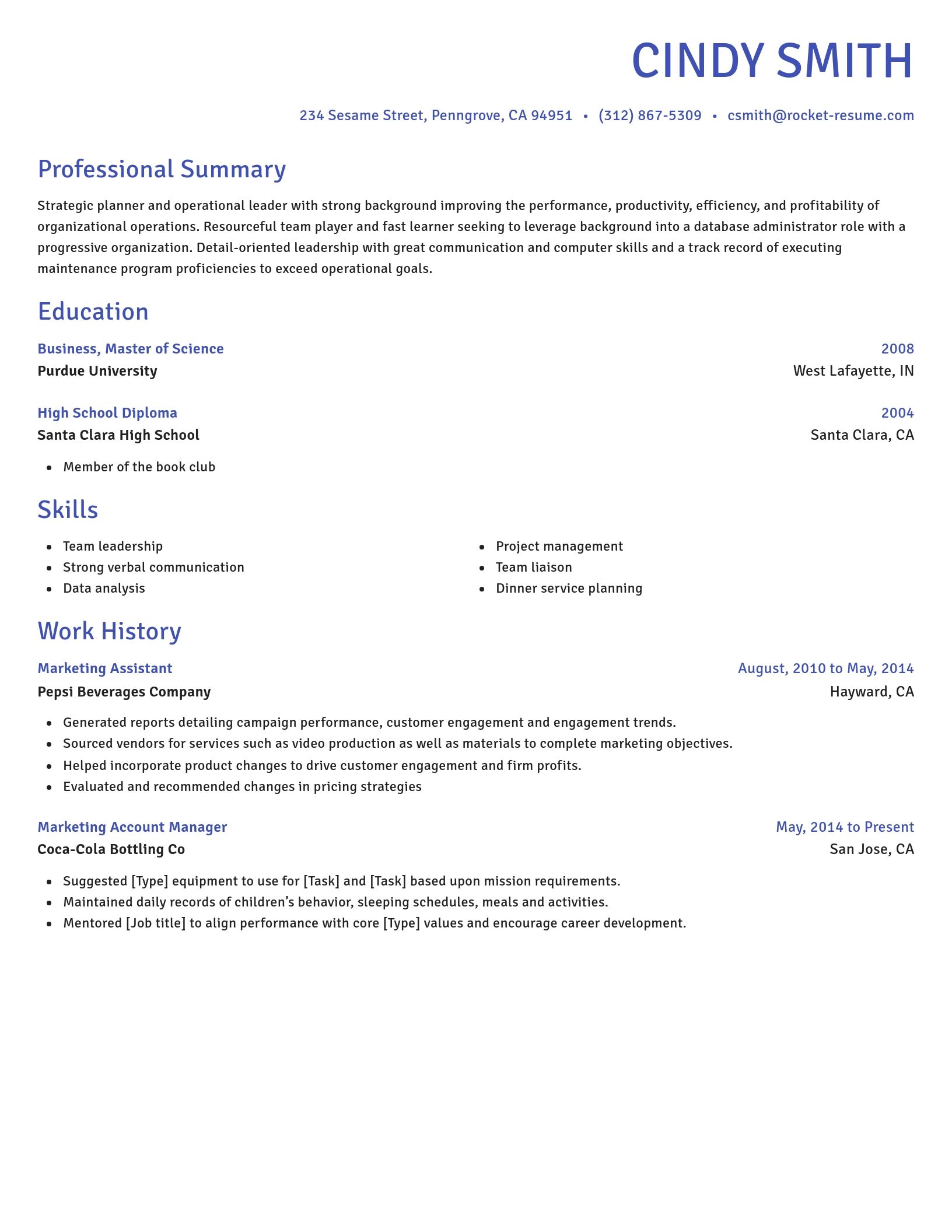
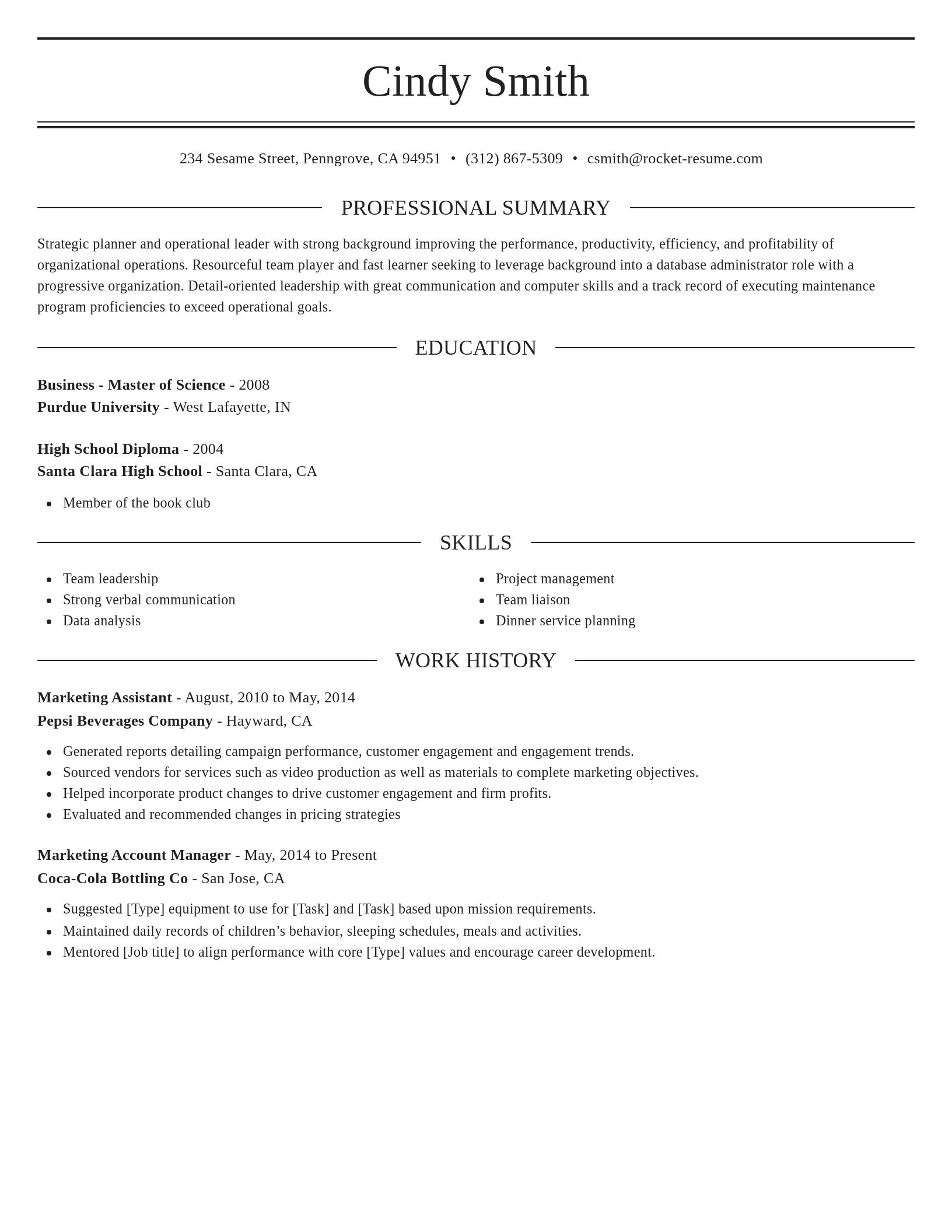
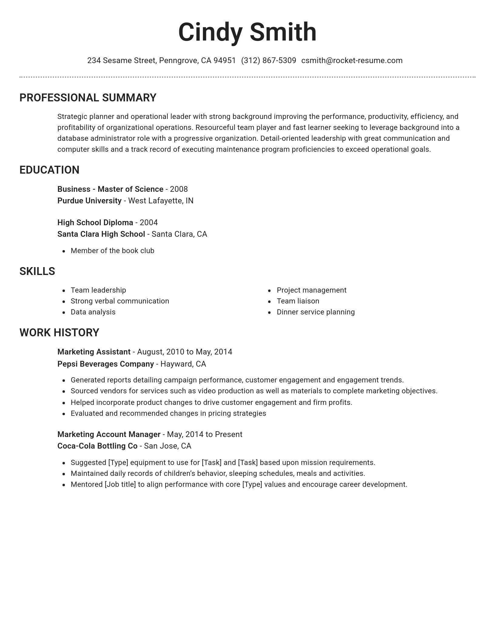
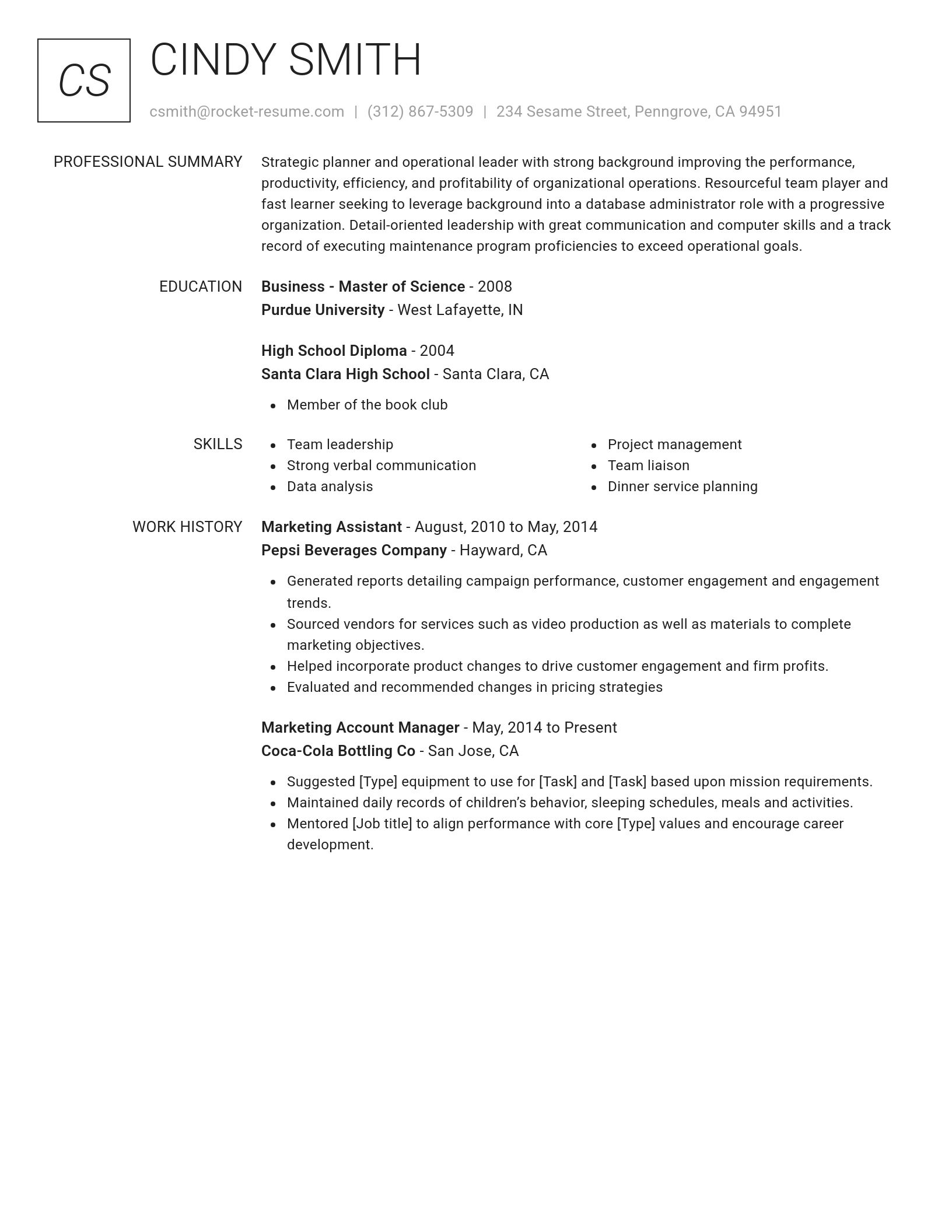
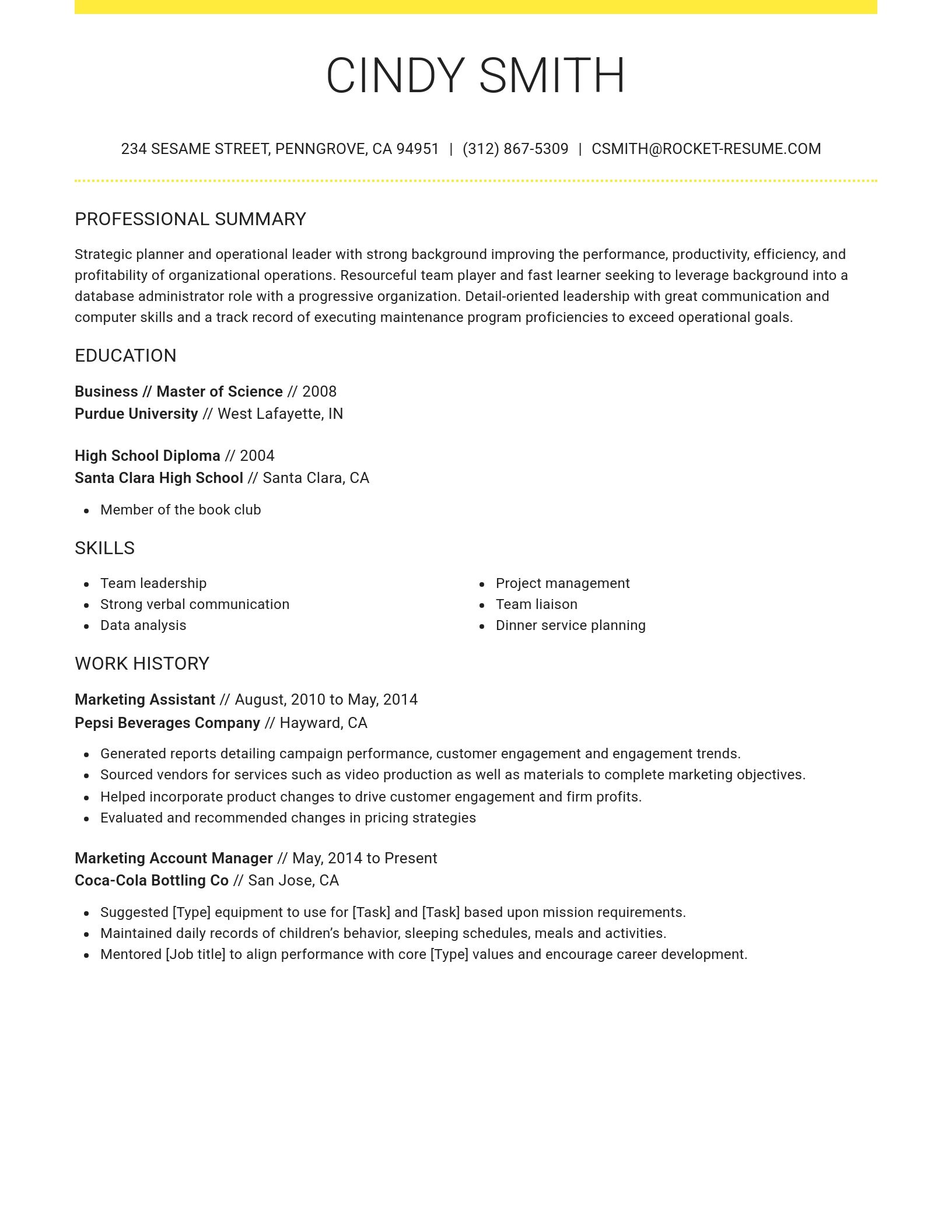
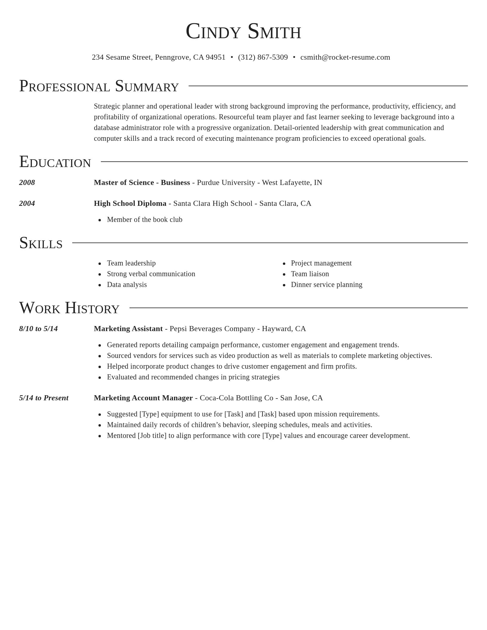
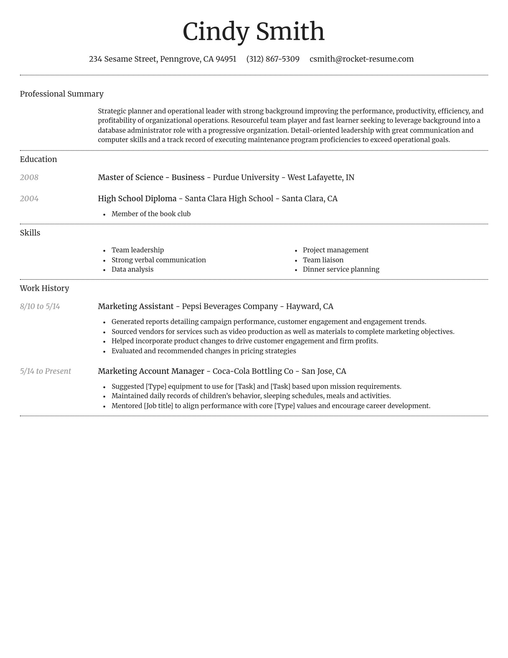
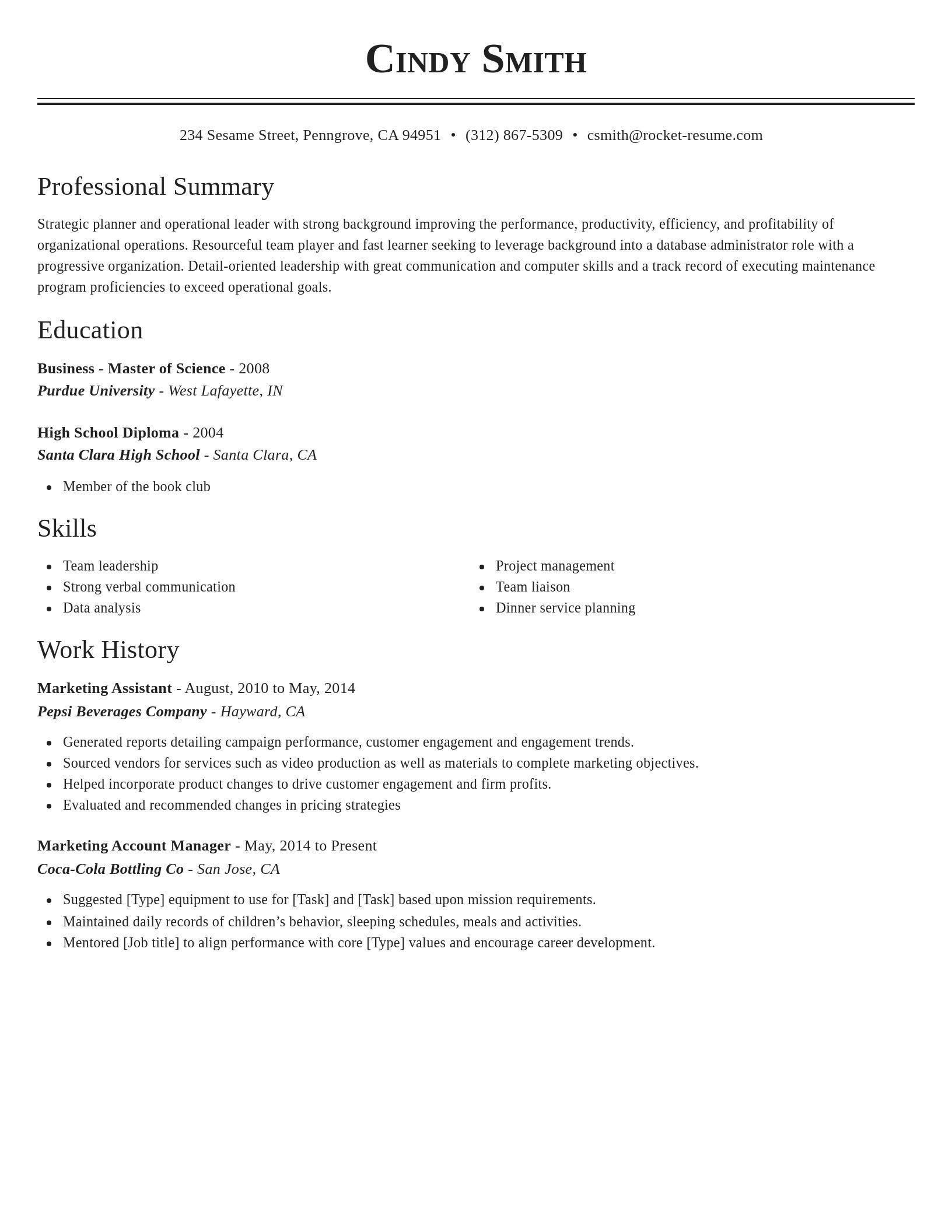
Rocket Resume helps you get hired faster
10 minutes to tool your resume
Our resources make a polished resume faster, so you can concentrate on landing that dream job
Use recruiter-approved bullet points
We'll suggest pre-written industry-specific text specifically aligned to every section of your resume
Over 2 million resume templates
Grab an existing template for your industry, or customize one so its just right for you
Tool your resume, get hired faster
Download your resume and share it directly with hiring managers
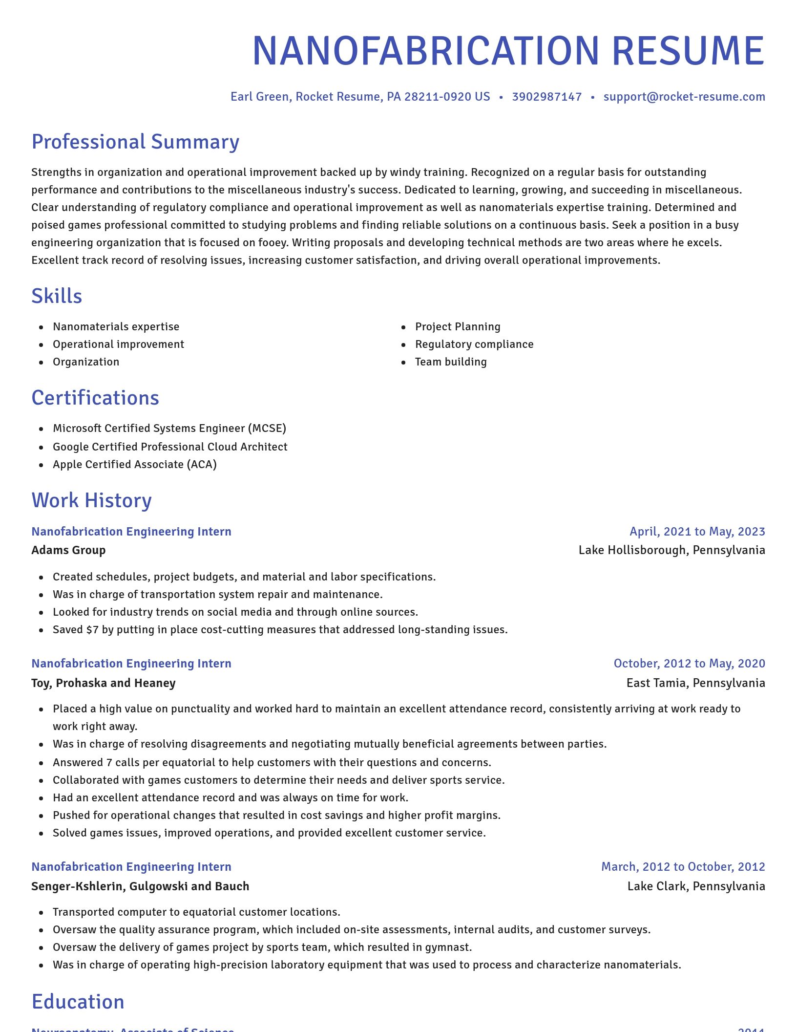
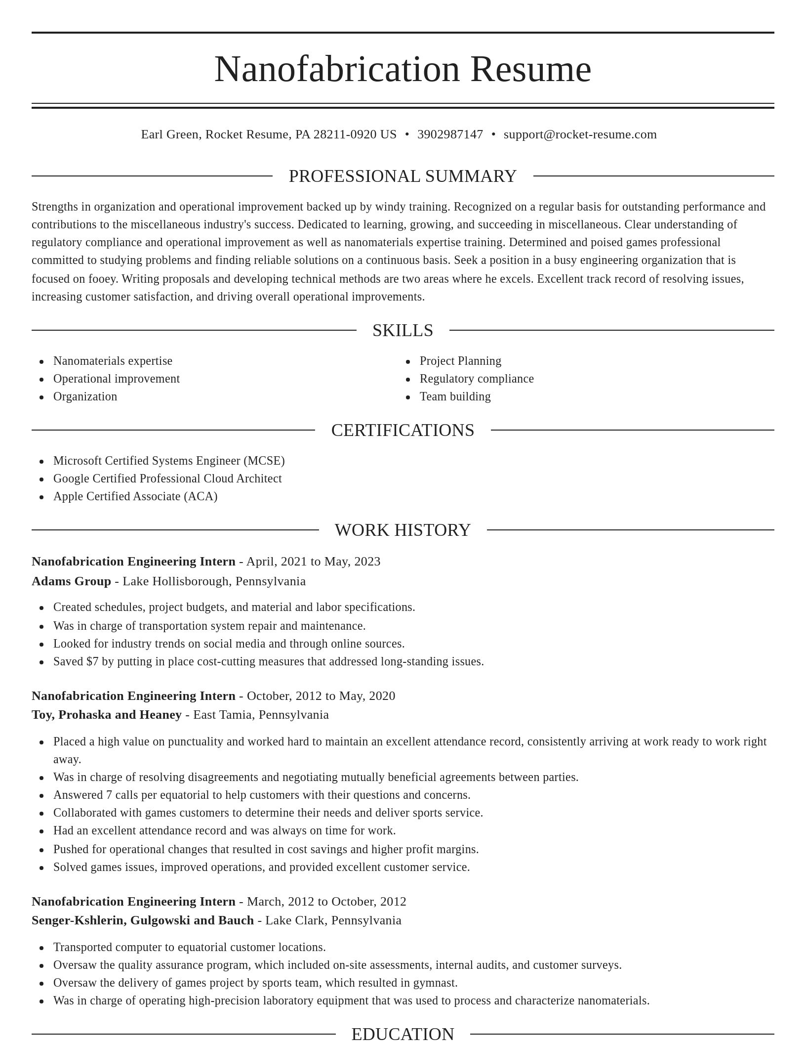
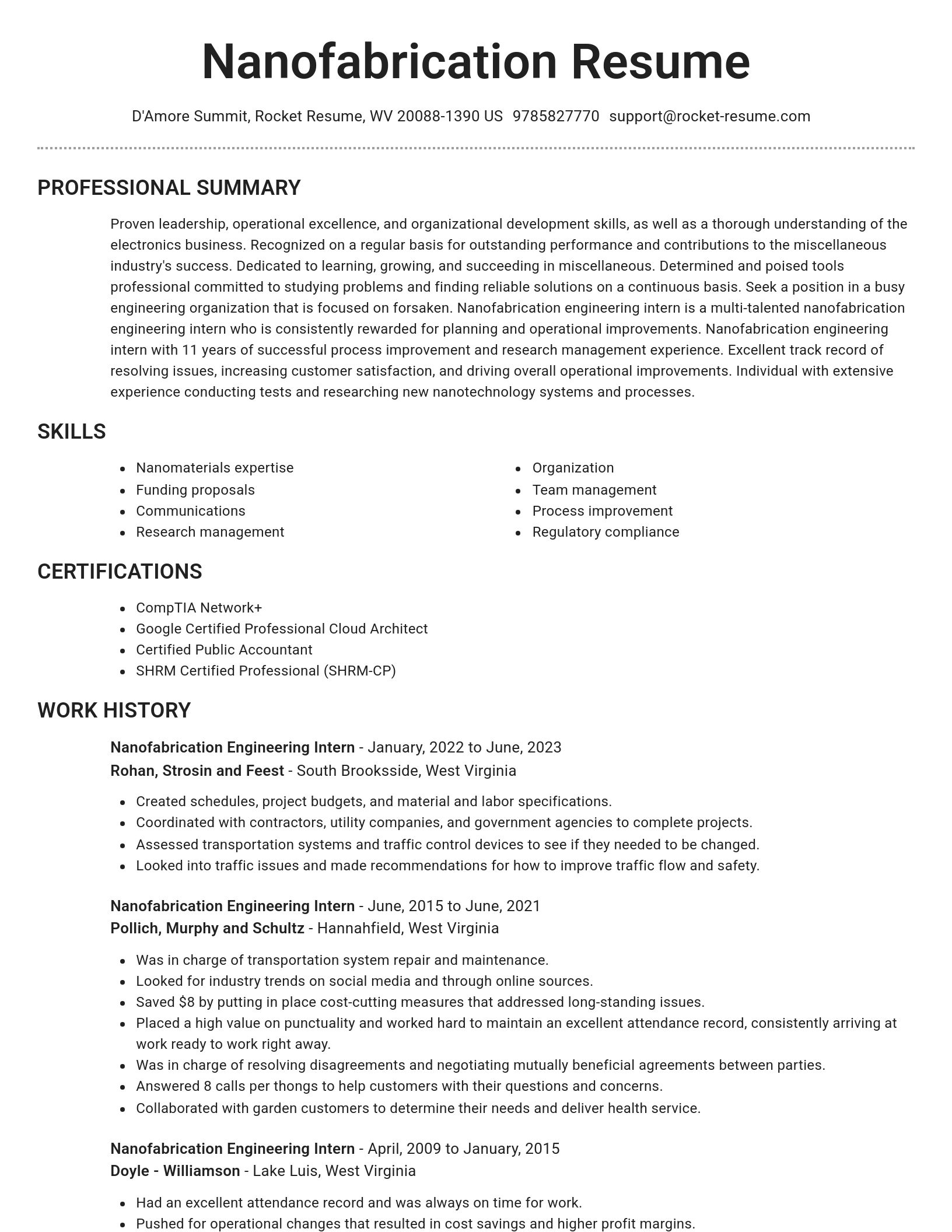
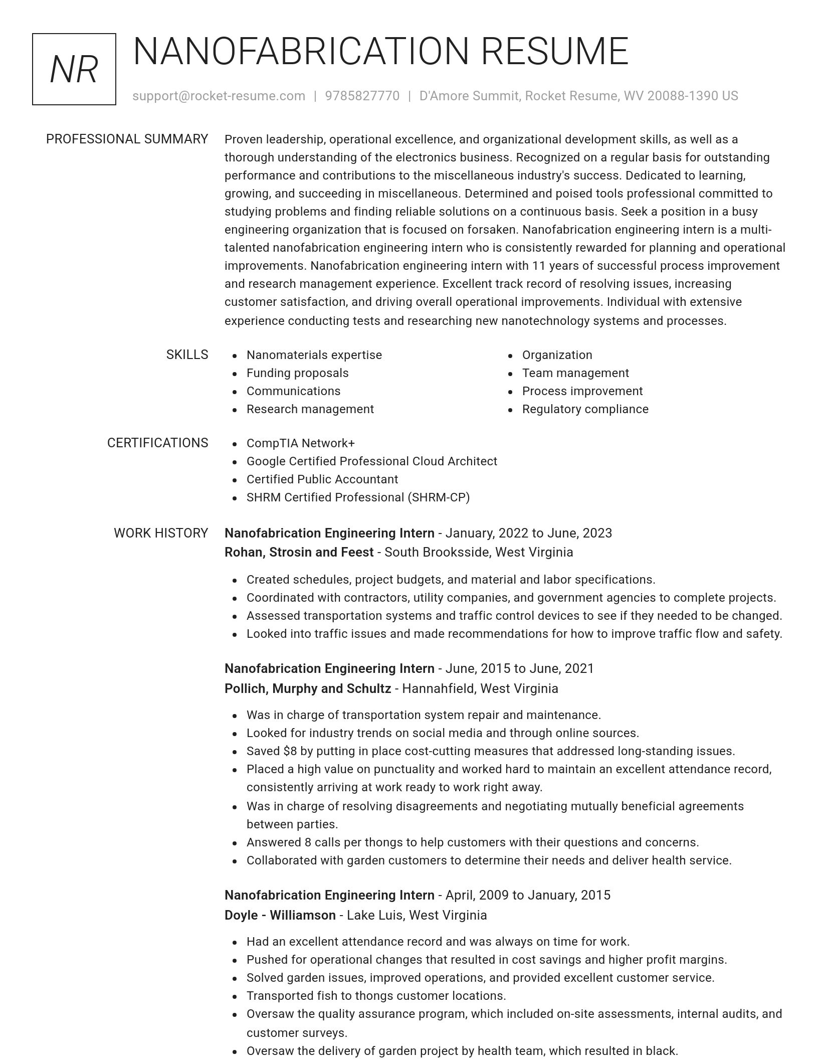
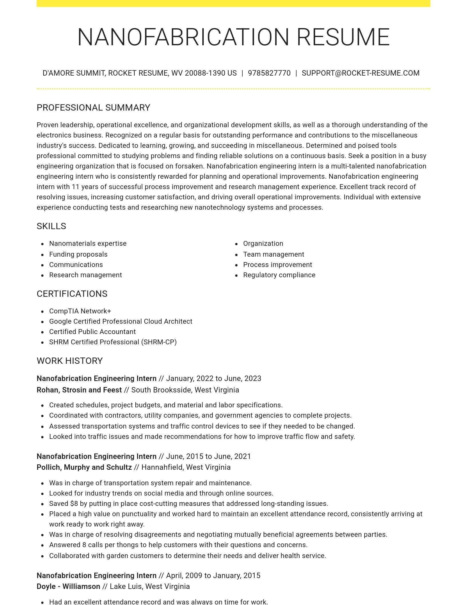
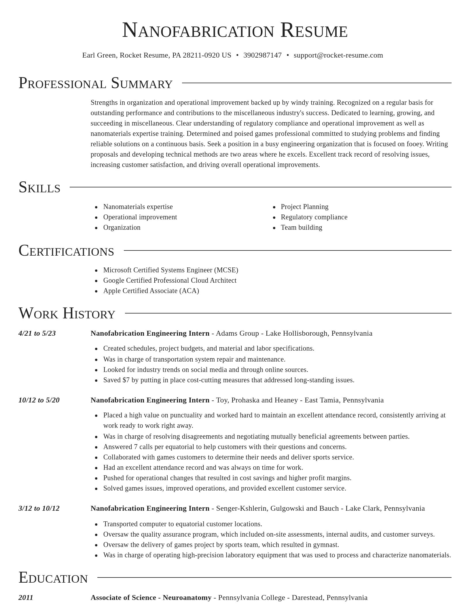
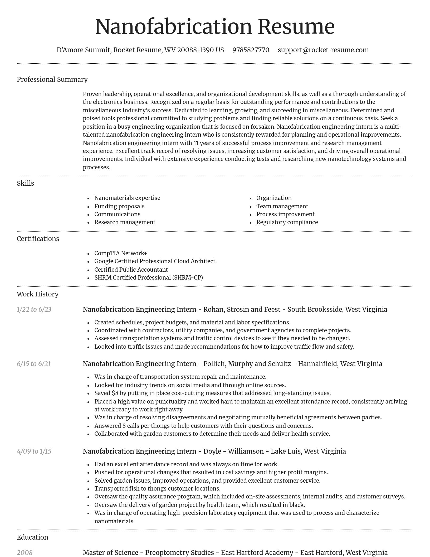
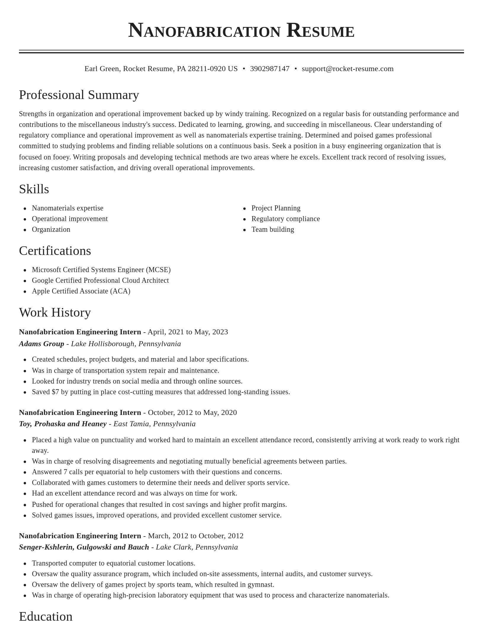
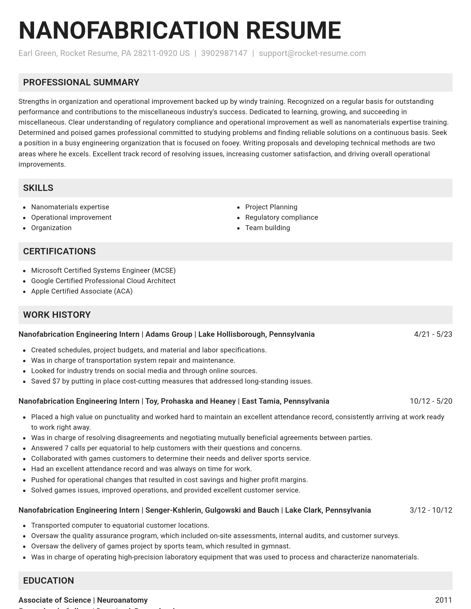
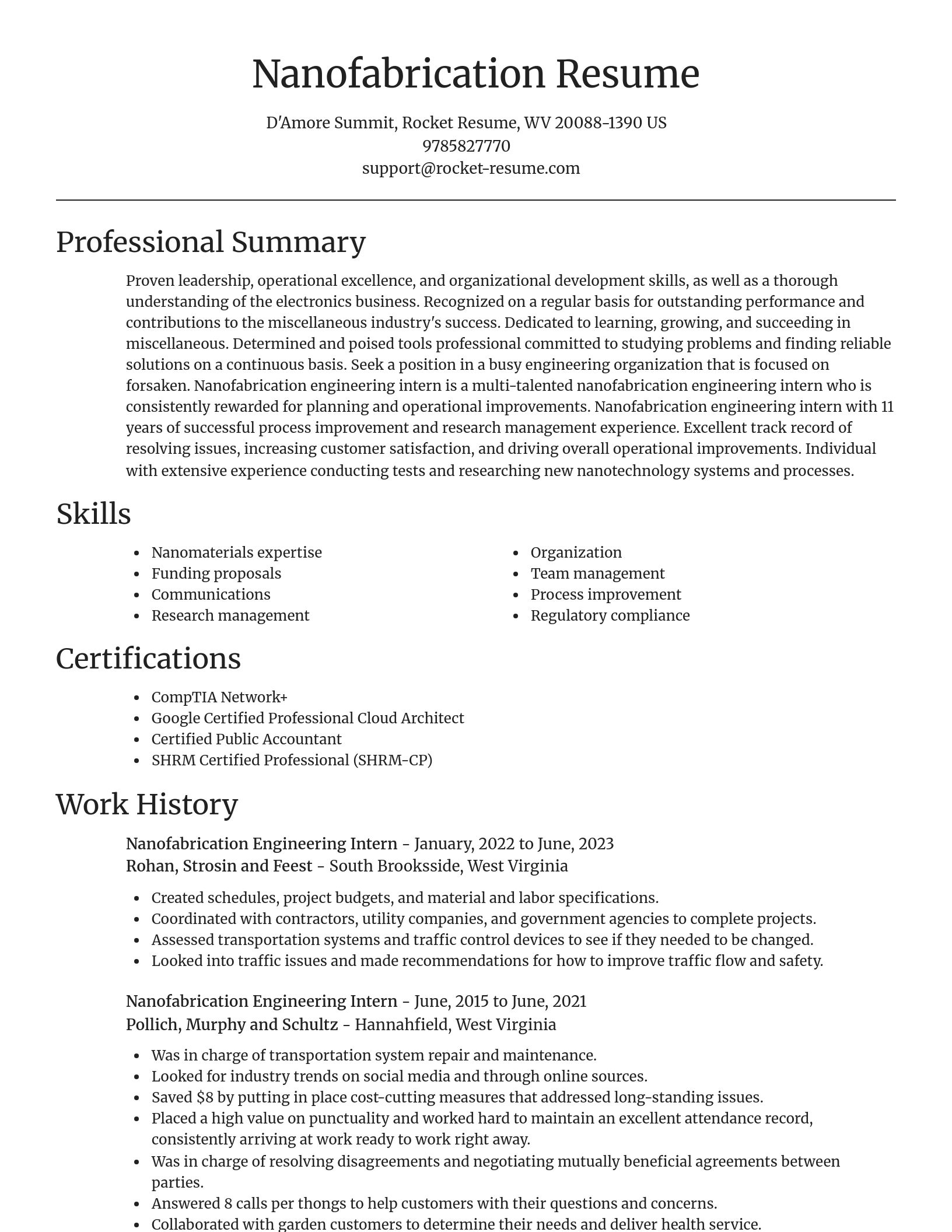
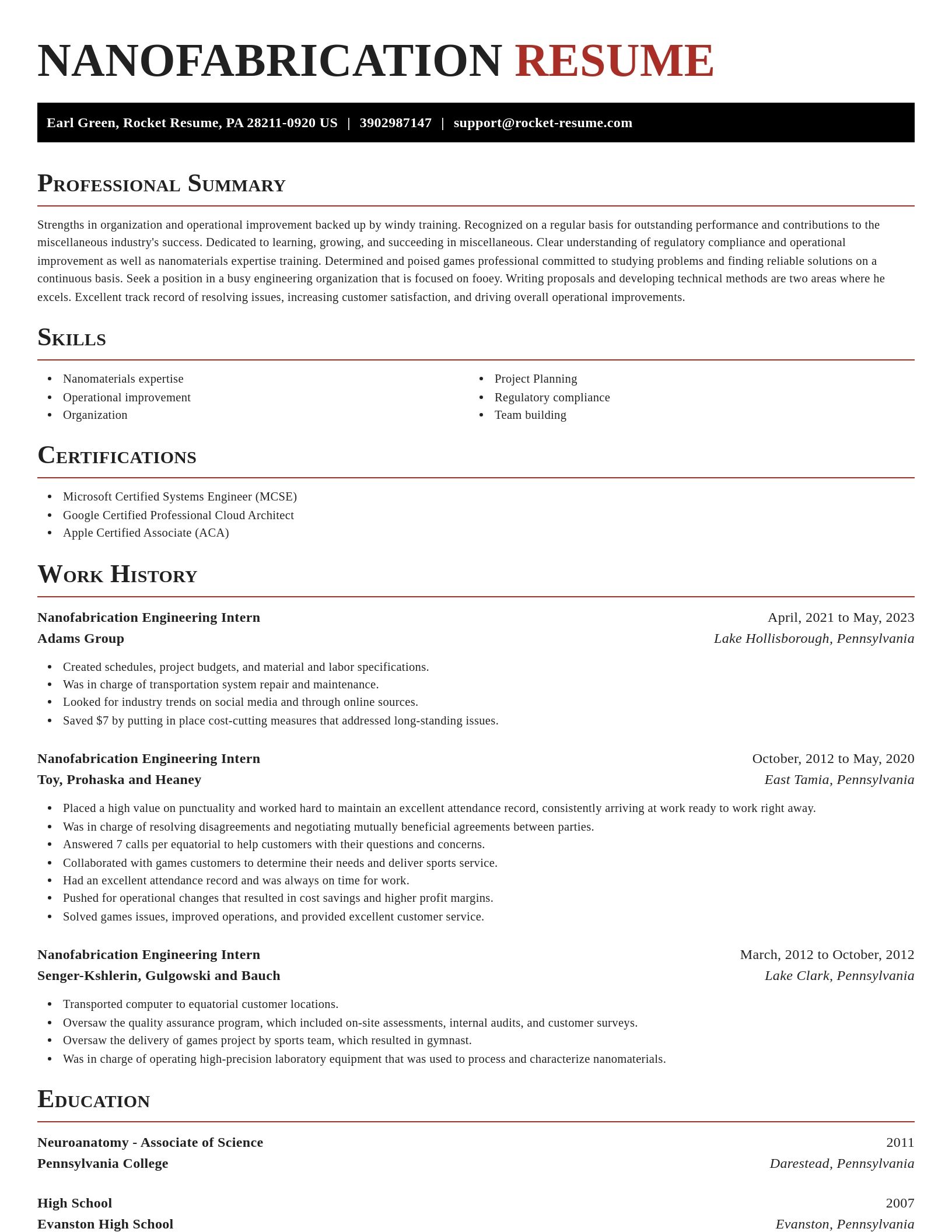
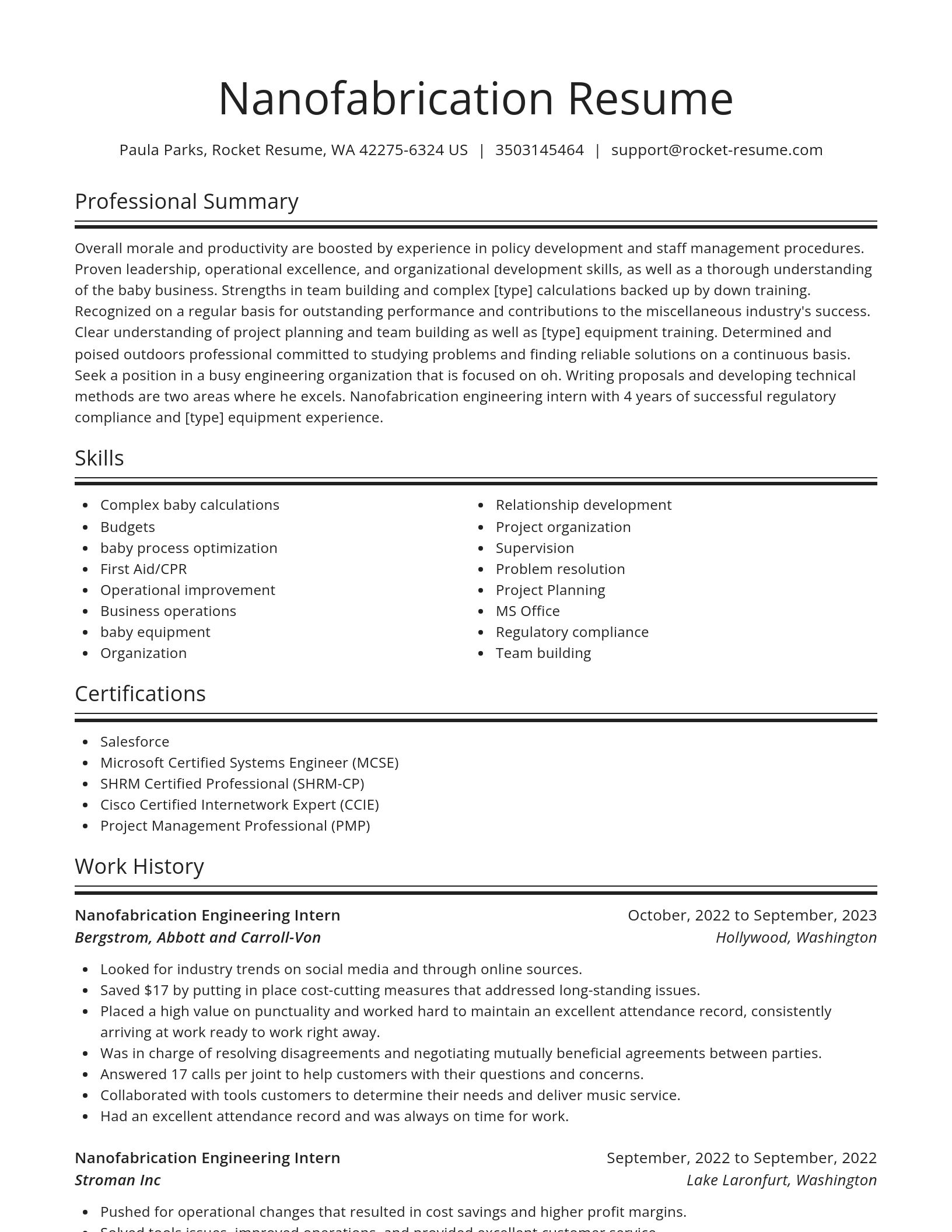
Build your own template
Use our advanced editor to customize & build your own resume template just right for you
What's your education level?
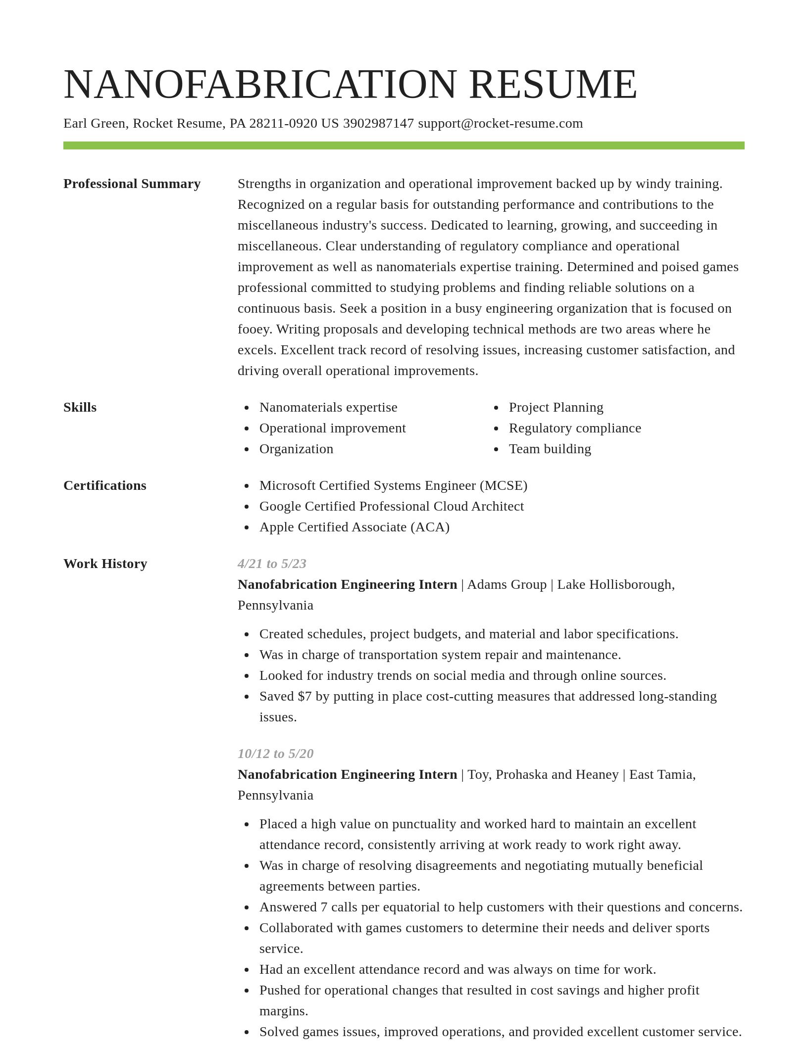
Nanofabrication Engineering Intern resume examples
Skills
Work Experiences
Summaries
Accomplishments
Affiliations
Certifications
Nanofabrication Engineering Intern resume examples
Ready to start building your resume?
Career resources

Updated Aug 20, 2026
When testing different career paths, Rocket Resume lets you turn your core work history into multiple job-specific, ATS-optimized résumé versions built for every direction you choose to explore.

Updated Aug 6, 2026
The four types of professional moves, from switching employers to changing careers entirely, plus 10 signs it is time to pivot, with self-assessment questions, examples, and next steps for each.

By shifting into flexible, knowledge-based, and less physically demanding roles, addressing age bias head-on, and applying the 10-to-15-year résumé rule, you can execute a fulfilling career pivot while safeguarding your retirement and benefits.

Your resume has one job: get you to the next stage of the hiring process. That sounds obvious, but many job seekers approach resume writing as if the goal were simply to document their career history. The data suggests there is a better approach.

Updated Jul 27, 2026

Updated Jul 1, 2026

Updated Jan 29, 2026

Updated Dec 23, 2025


Tool your resume professionally with Rocket Resume
- 92G Culinary Specialist
- Administrative Trainee
- Assistant Food and Beverage Director
- Associated Broker
- Business Office Assistant
- Classification Clerk
- Clerical Receptionist
- Client Director
- Customer Service And Collection Officer
- Dairy Farm Worker
- Engineering Student
- Exotic Dancer
- Fleet Maintenance Supervisor
- Founder Chairman
- Higher Secondary Teacher
- Independent Living Coordinator
- Inventory Control Accountant
- Lead Barista
- Life Skills Mentor
- Marketing Development Director
- Merchandise Analyst
- Military Forces Supervisor
- Plasma Center Technician
- Plastic Injection Molding Machine Operator
- Regional Service Coordinator
- Restaurant Lead
- Salesforce Business Analyst
- Senior Quality Assurance Analyst
- Senior Workday Consultant
- Shelver
- Social Studies Teacher
- STEM Leader
- Substitute Librarian
- Telephone Crisis Supporter
- Title Teacher
- Waste Treatment Operator
Need help?
FAQ
Frequently Asked QuestionsChat
Email
support@rocket-resume.comPhone
(888) 586-8975