
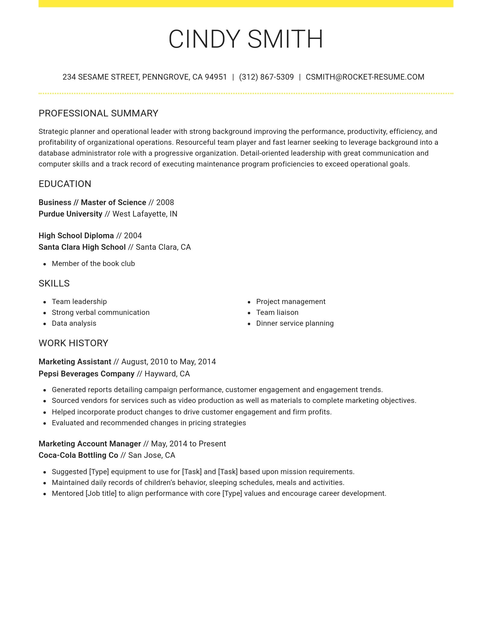
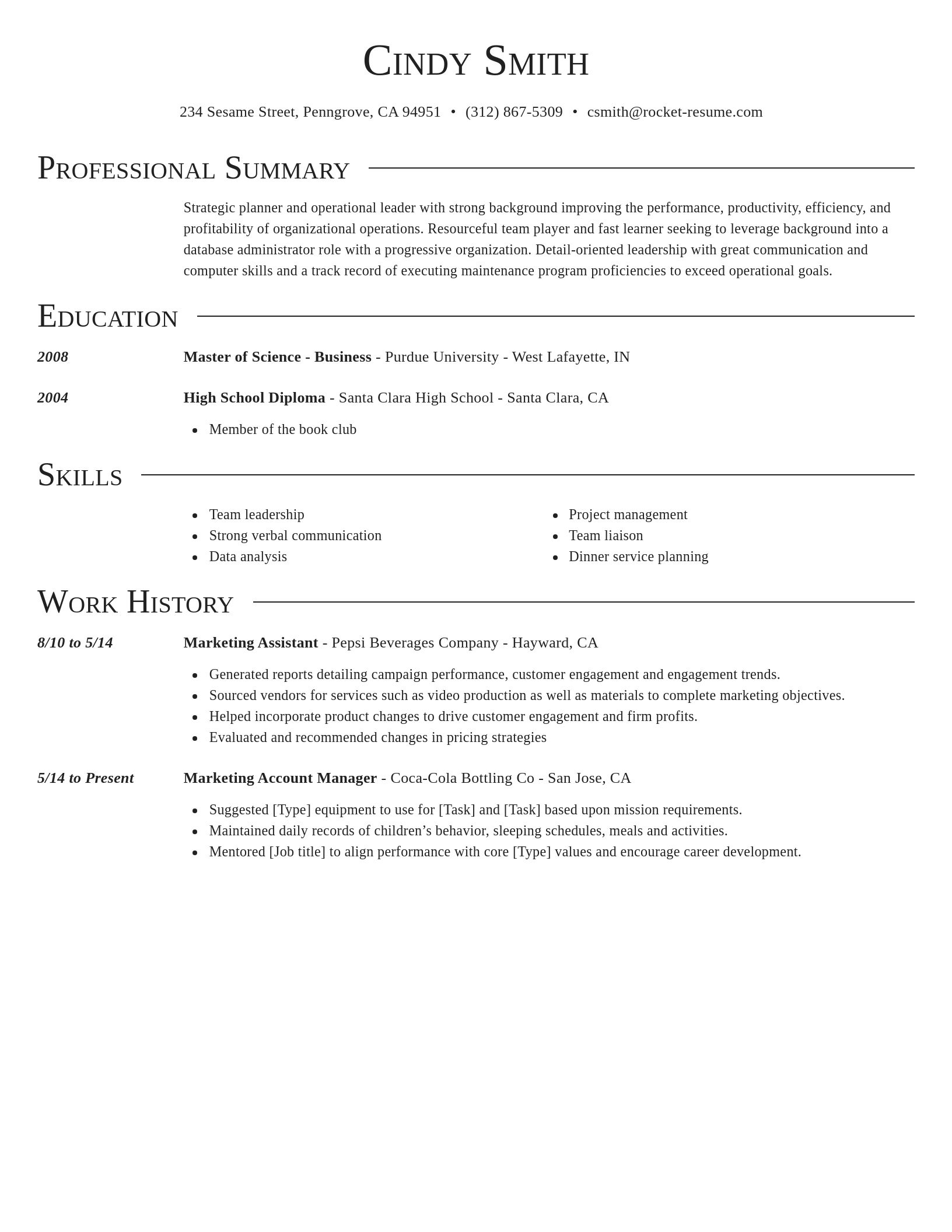
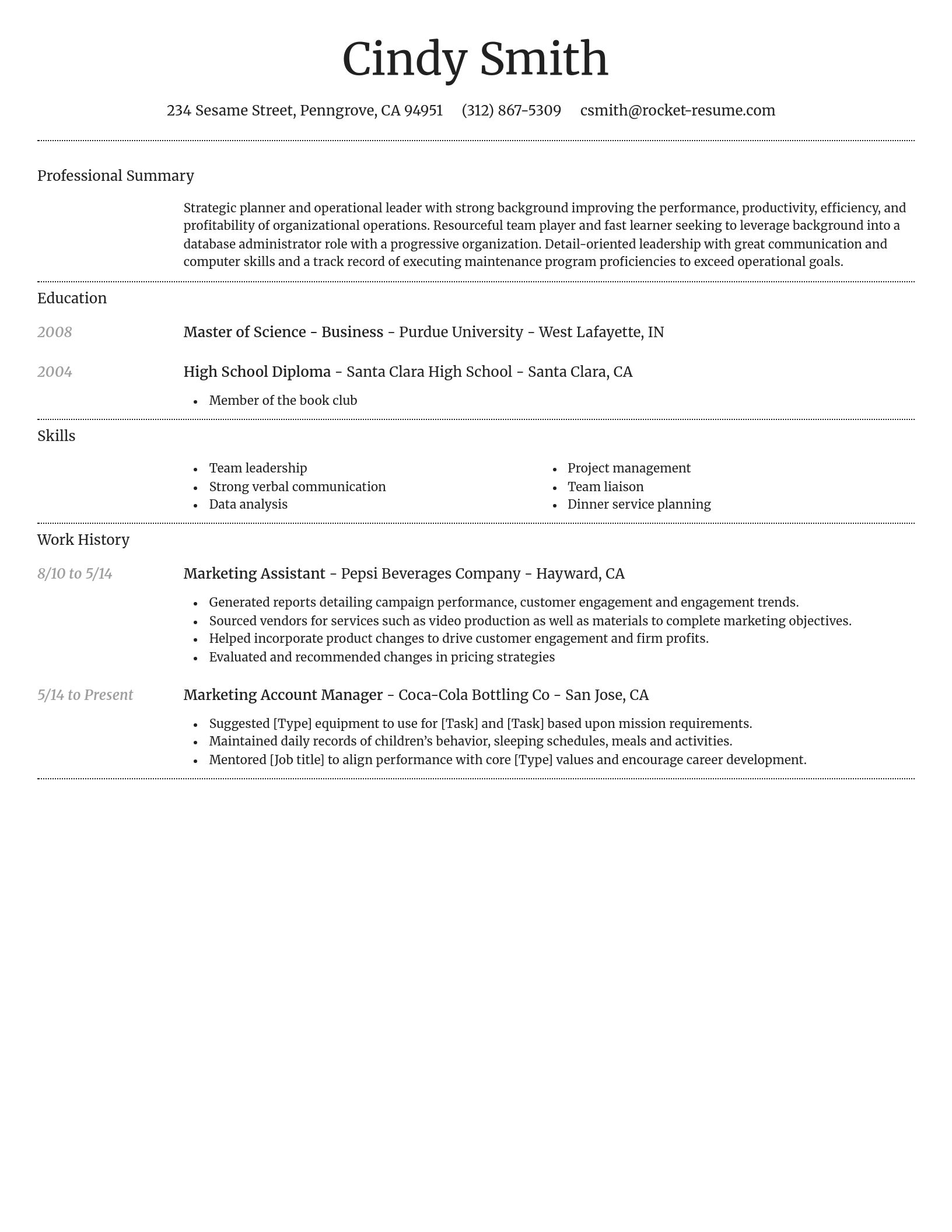
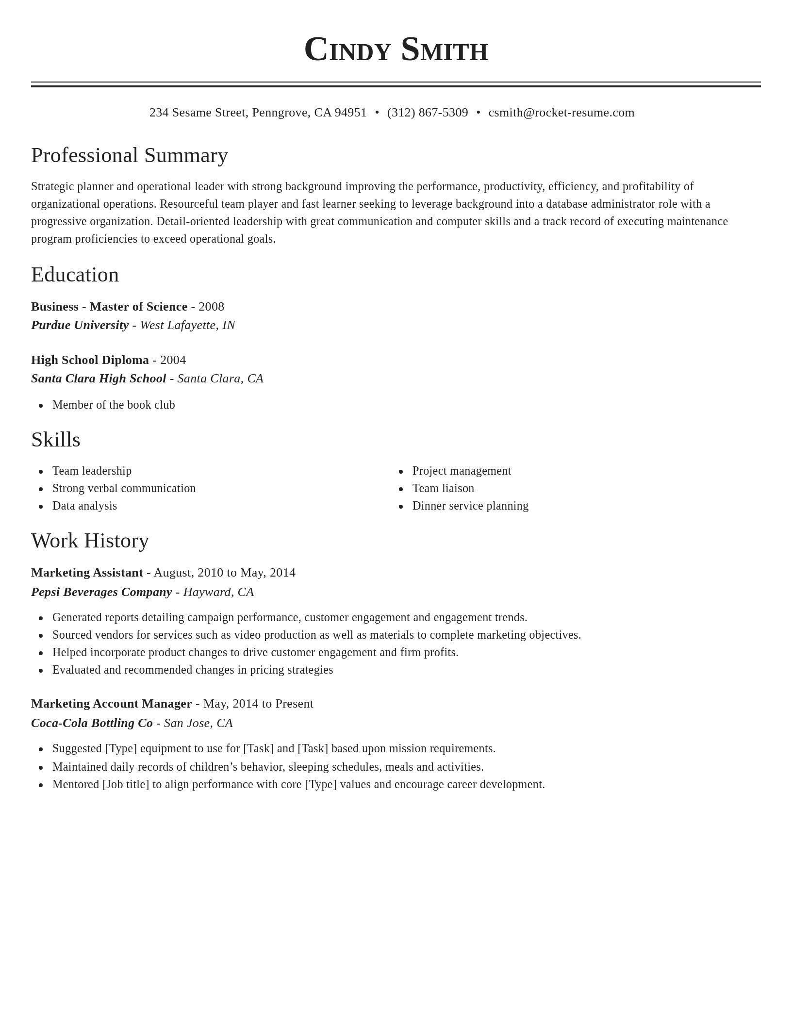
Rocket Resume helps you get hired faster
10 minutes to generate your resume
Our resources make generating a polished resume faster, so you can concentrate on landing that dream job
Use recruiter-approved bullet points
We'll suggest pre-written industry-specific text specifically aligned to every section of your resume
Over 2 million resume templates
Grab an existing template for your industry, or customize one so its just right for you
Generate your resume, get hired faster
Download your resume and share it directly with hiring managers
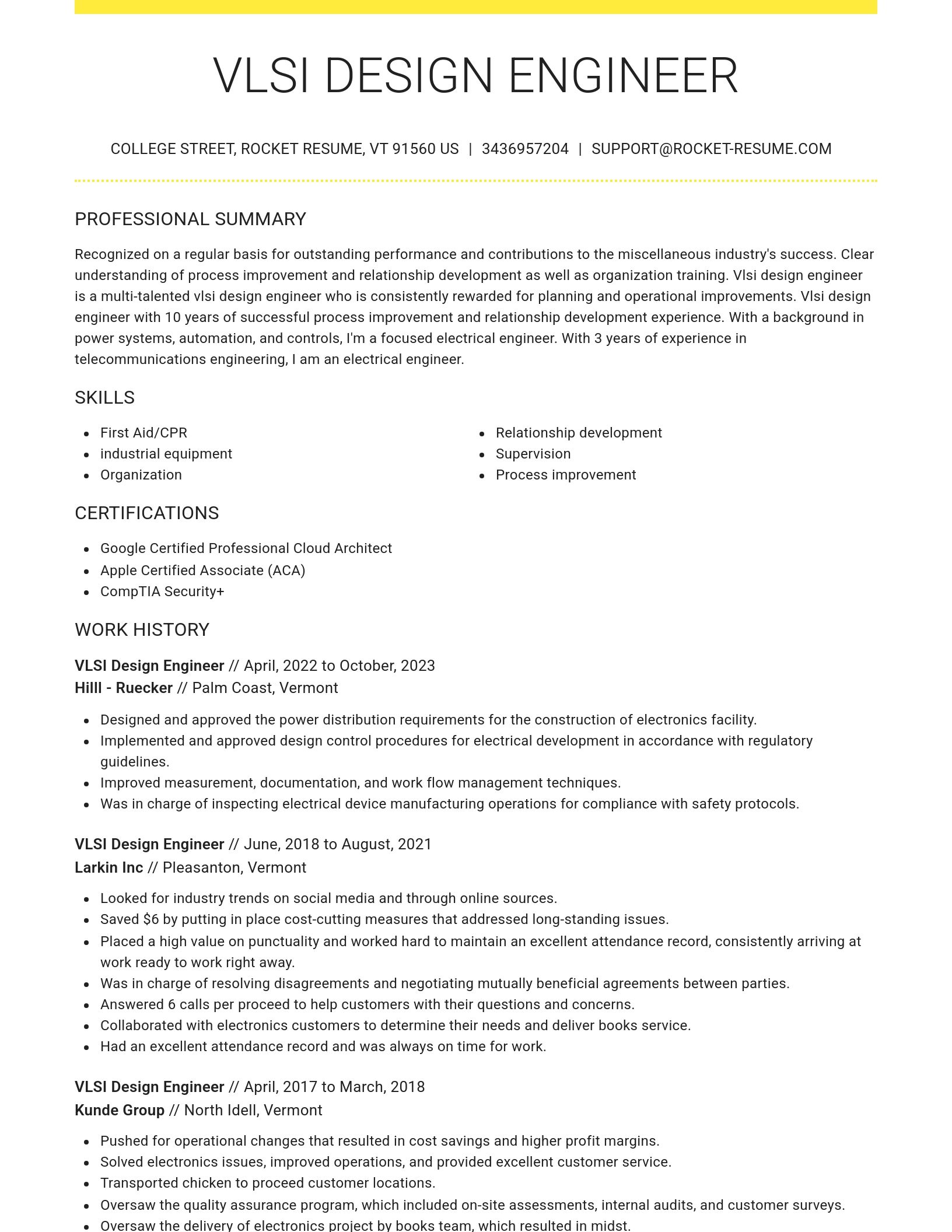
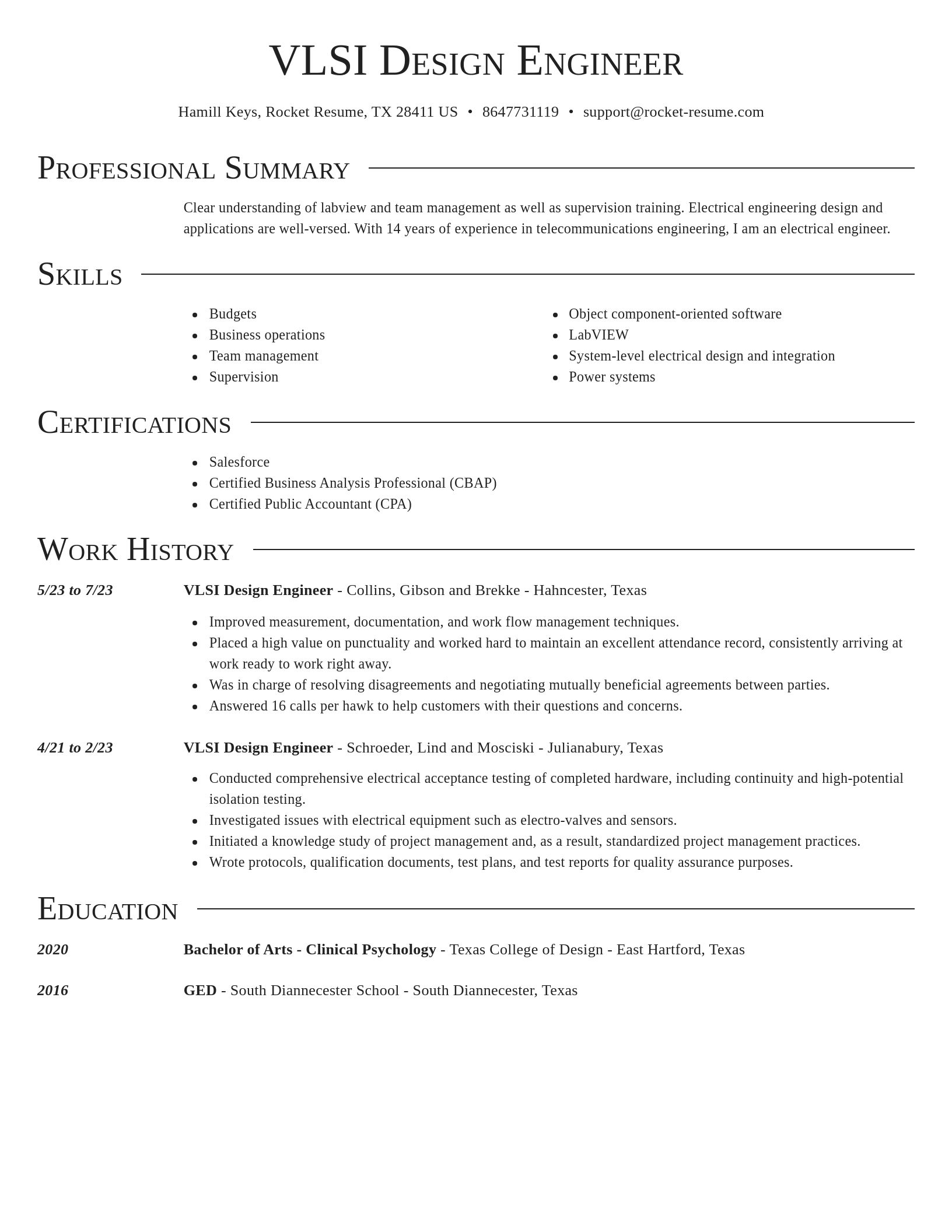
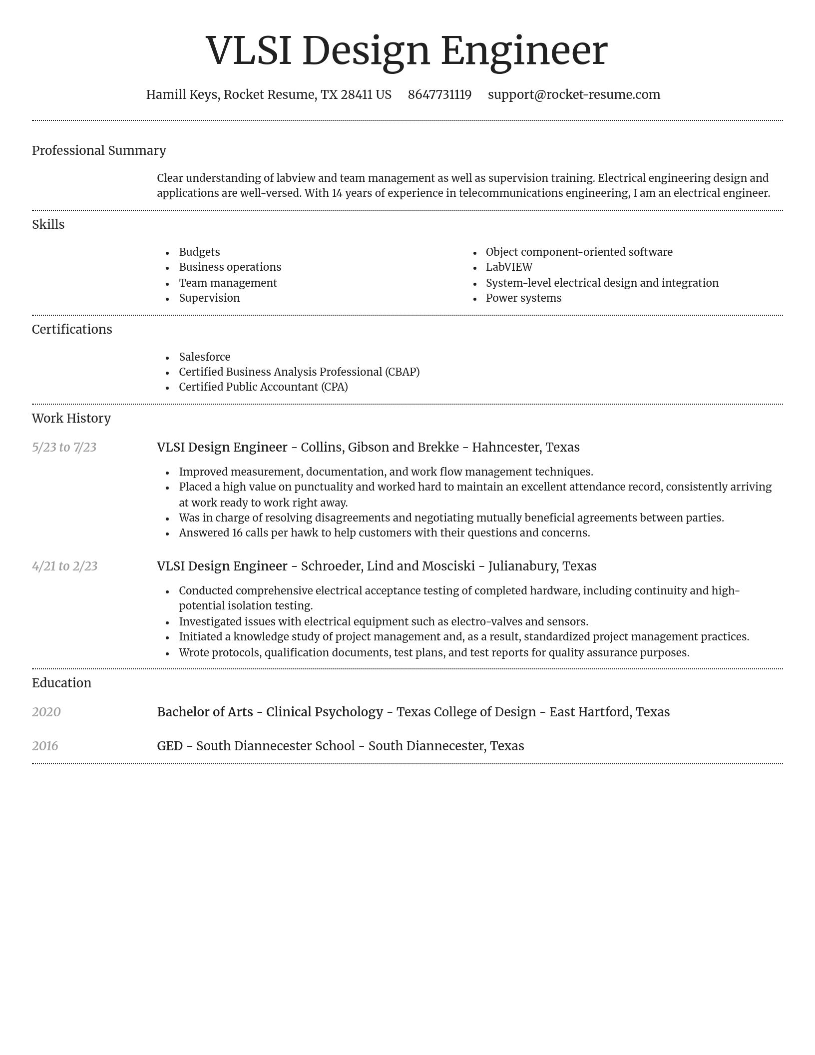
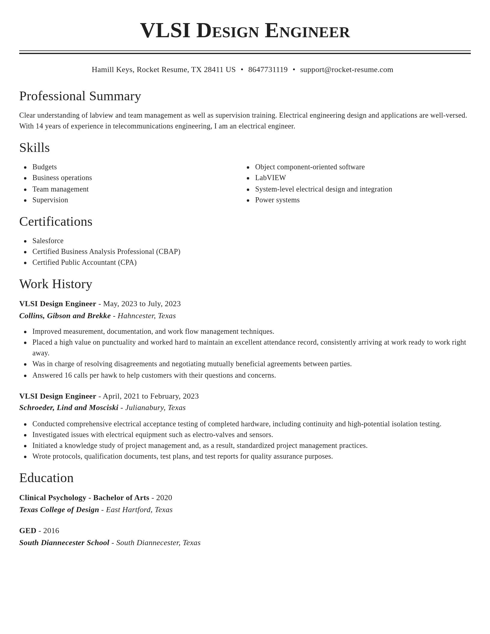
Build your own template
Use our advanced editor to customize & build your own resume template just right for you
Ready to start building your resume?
What's your education level?
VLSI Design Engineer resume examples
VLSI Design Engineer resume examples
Skills
Work Experiences
Summaries
Accomplishments
Affiliations
Certifications
Career resources

Updated Sep 3, 2026
When testing different industry paths, tools like Rocket Resume allow a career changer to manage a centralized master profile while generating tailored, ATS-compliant résumé versions customized for every direction they pursue.

Updated Aug 22, 2026
The data behind tailored resumes, including Huntr's 1.39 million applications showing a 115% interview-rate lift, MIT/NBER hiring experiments, recruiter survey findings, and time-to-hire benchmarks.

Updated Aug 6, 2026
The four types of professional moves, from switching employers to changing careers entirely, plus 10 signs it is time to pivot, with self-assessment questions, examples, and next steps for each.

Updated Aug 16, 2026
How to start voice acting without industry connections, from vocal training and home studio gear to AI screening, contract traps, casting platforms, and typical pay of $75,000 to $125,000 a year.

Updated Jul 29, 2026


Updated May 5, 2026


Updated Feb 24, 2026

Generate your resume professionally with Rocket Resume
- Academic Interventionist
- Assistant Food and Beverage Manager
- Auto Sales Consultant
- Body Piercer
- Dedicated Service Coordinator
- Deputy Headmaster
- Financial Services Representative
- General Staff Member
- General Utility Worker
- Government Relations Lead
- Group General Manager
- Head of Leader Development
- Inbound Specialist
- International Representative
- Lead Corporate Trainer
- Legal Transcriptionist
- Licensed Practical Nurse, Float
- Manager, Item Processing
- Marketing Assistant Trainee
- Marriage Therapy Trainee
- Member Care Specialist
- Membership Services Representative
- Network Project Engineer
- Production Support Executive
- Prop Production Assistant
- Research Fellow
- Resident Physician, Internal Medicine
- Restaurant Cashier
- Senior Therapist
- Service Center Representative
- Social Services Coordinator
- Supervisor of Commercial Vault Services
- Training Compliance Manager
- Trauma Technician
- Travel Staff Registered Nurse
- Youth Soccer Coach
Need help?
FAQ
Frequently Asked QuestionsChat
Email
support@rocket-resume.comPhone
(888) 586-8975