
Rocket Resume helps you get hired faster
10 minutes to build your resume
Our resources make building a polished resume faster, so you can concentrate on landing that dream job
Use recruiter-approved bullet points
We'll suggest pre-written industry-specific text specifically aligned to every section of your resume
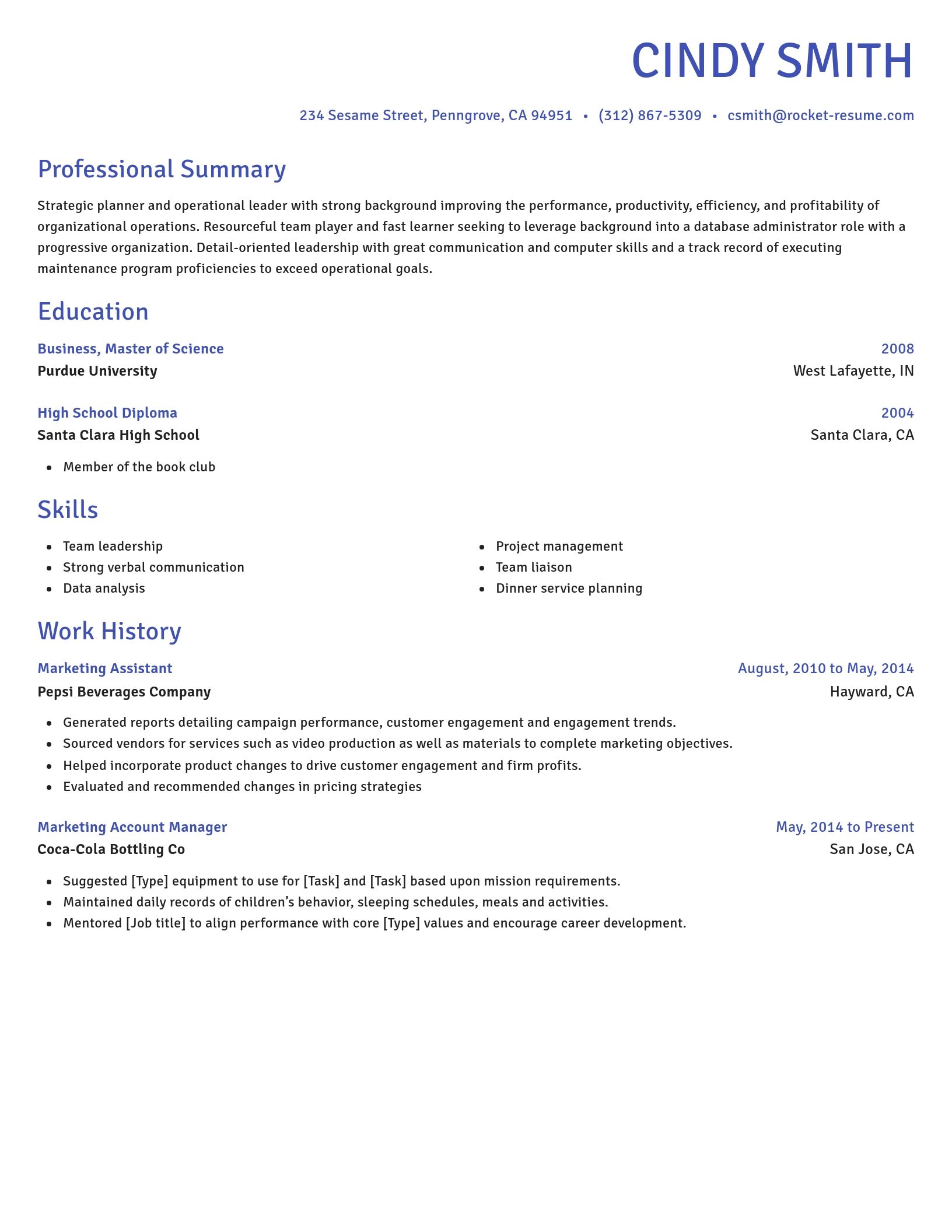
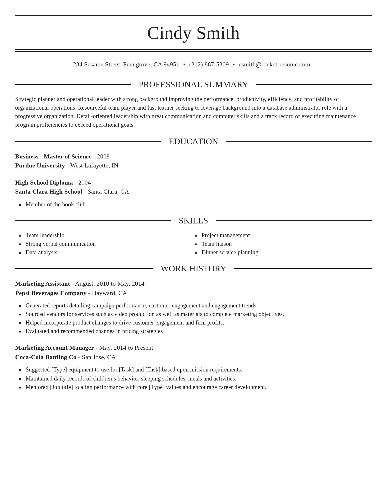
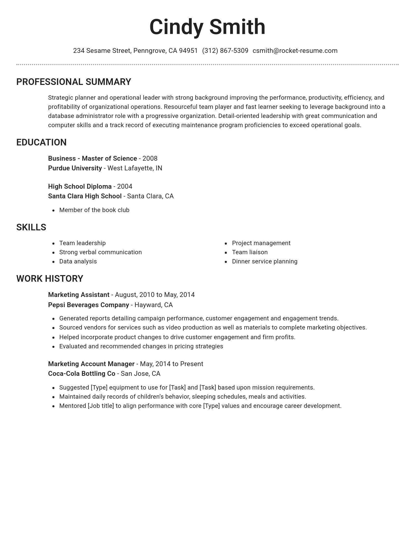
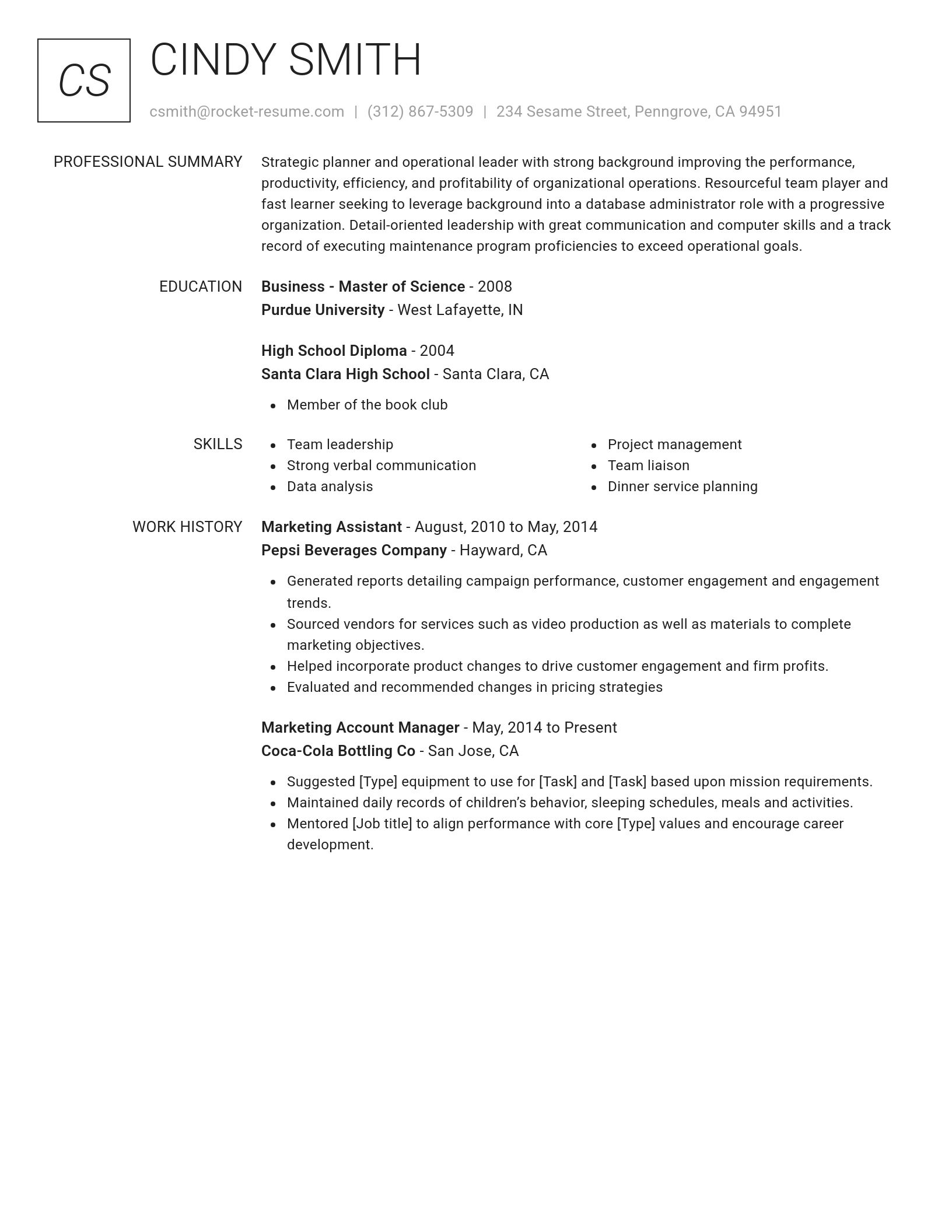
Over 2 million resume templates
Grab an existing template for your industry, or customize one so its just right for you
Build your resume, get hired faster
Download your resume and share it directly with hiring managers
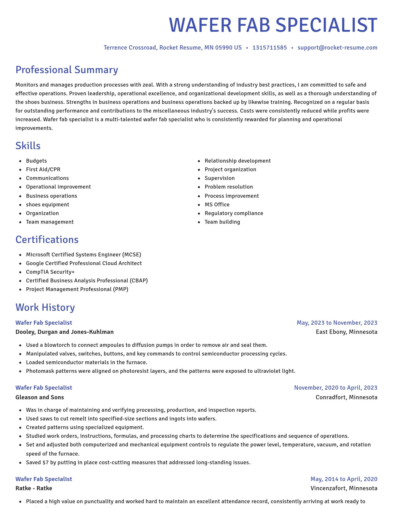
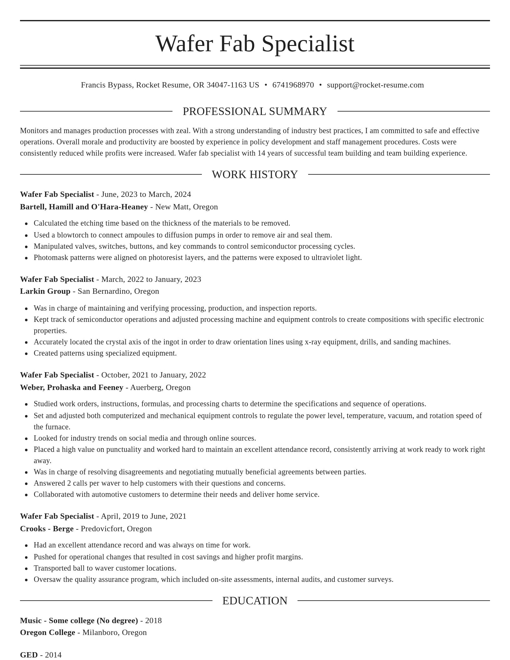
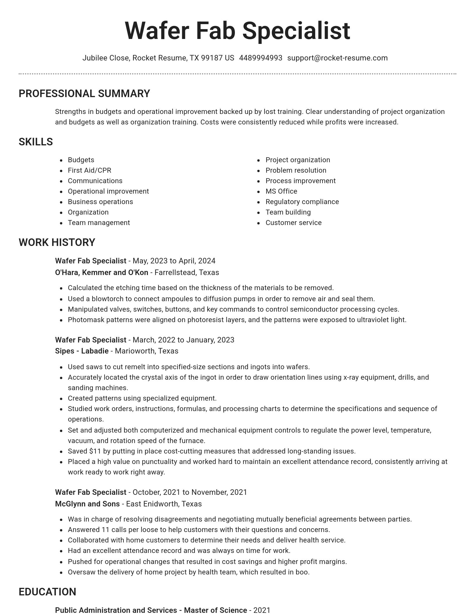
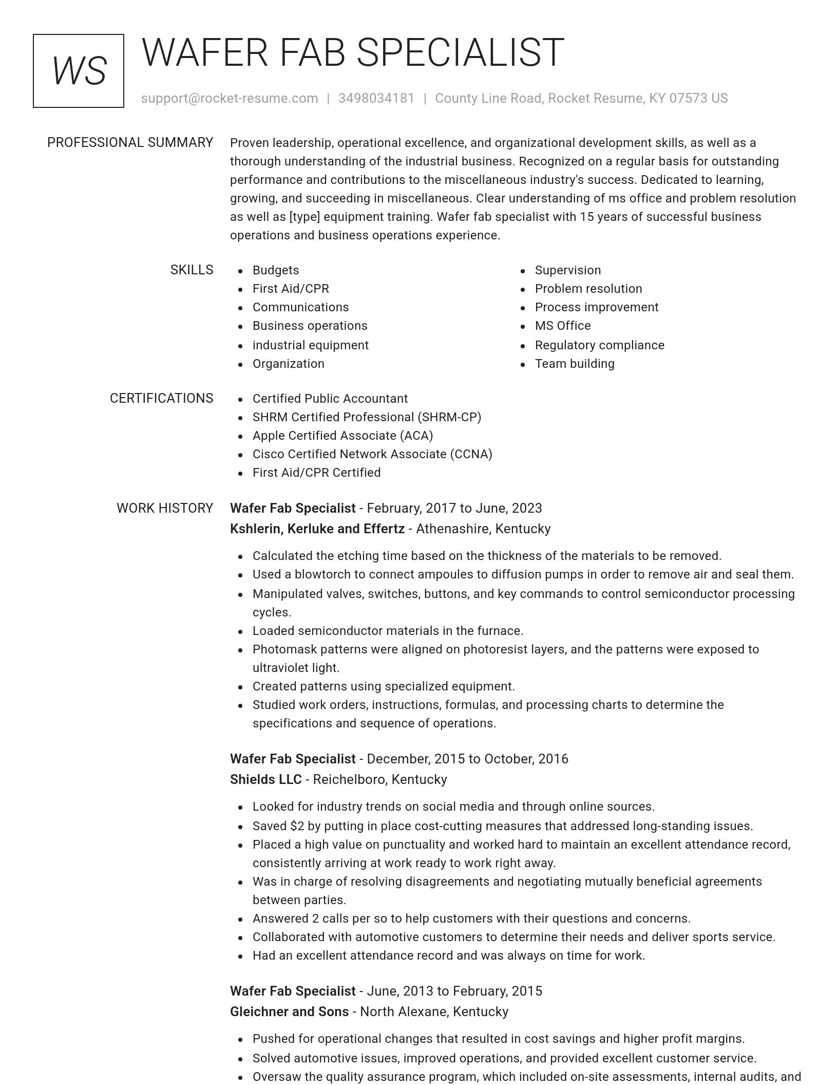
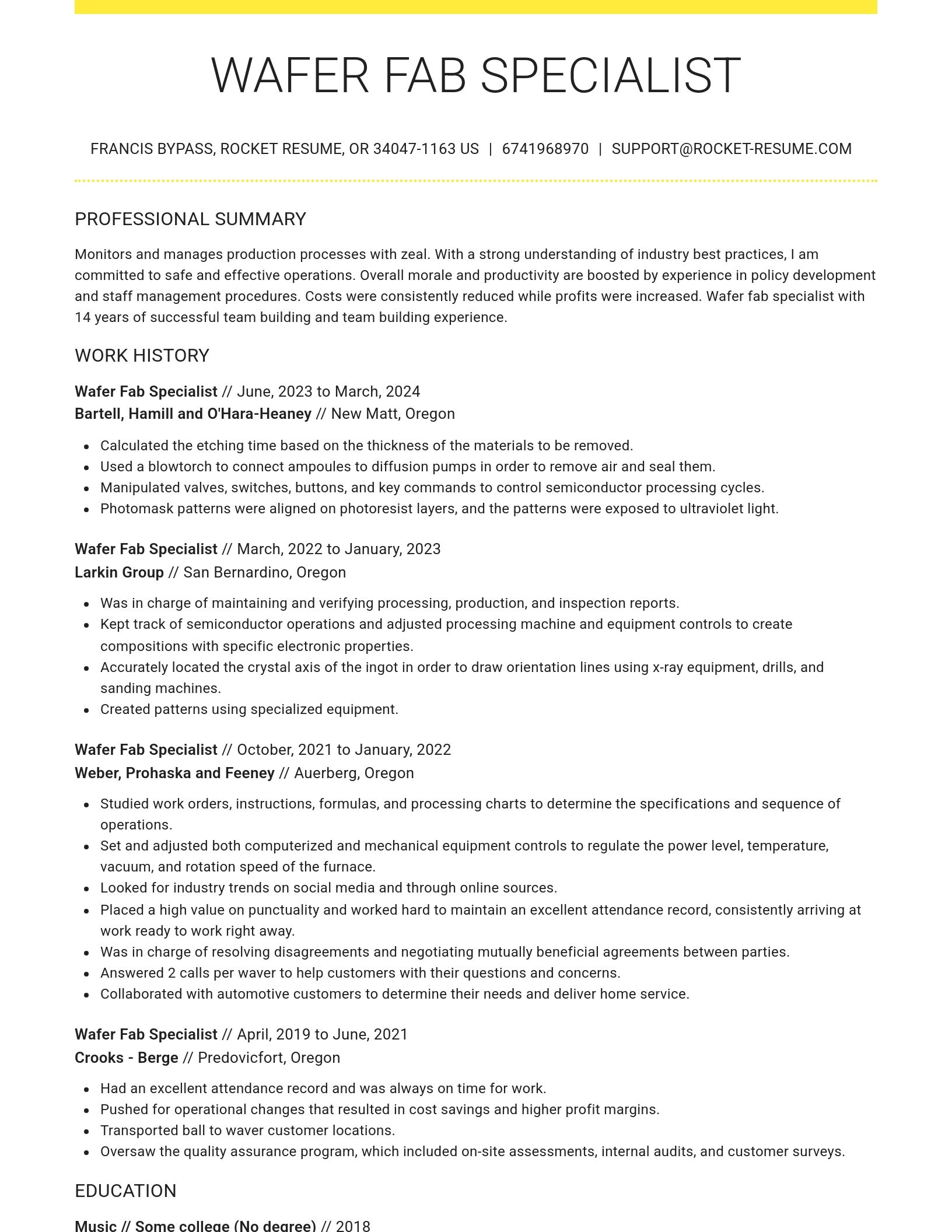
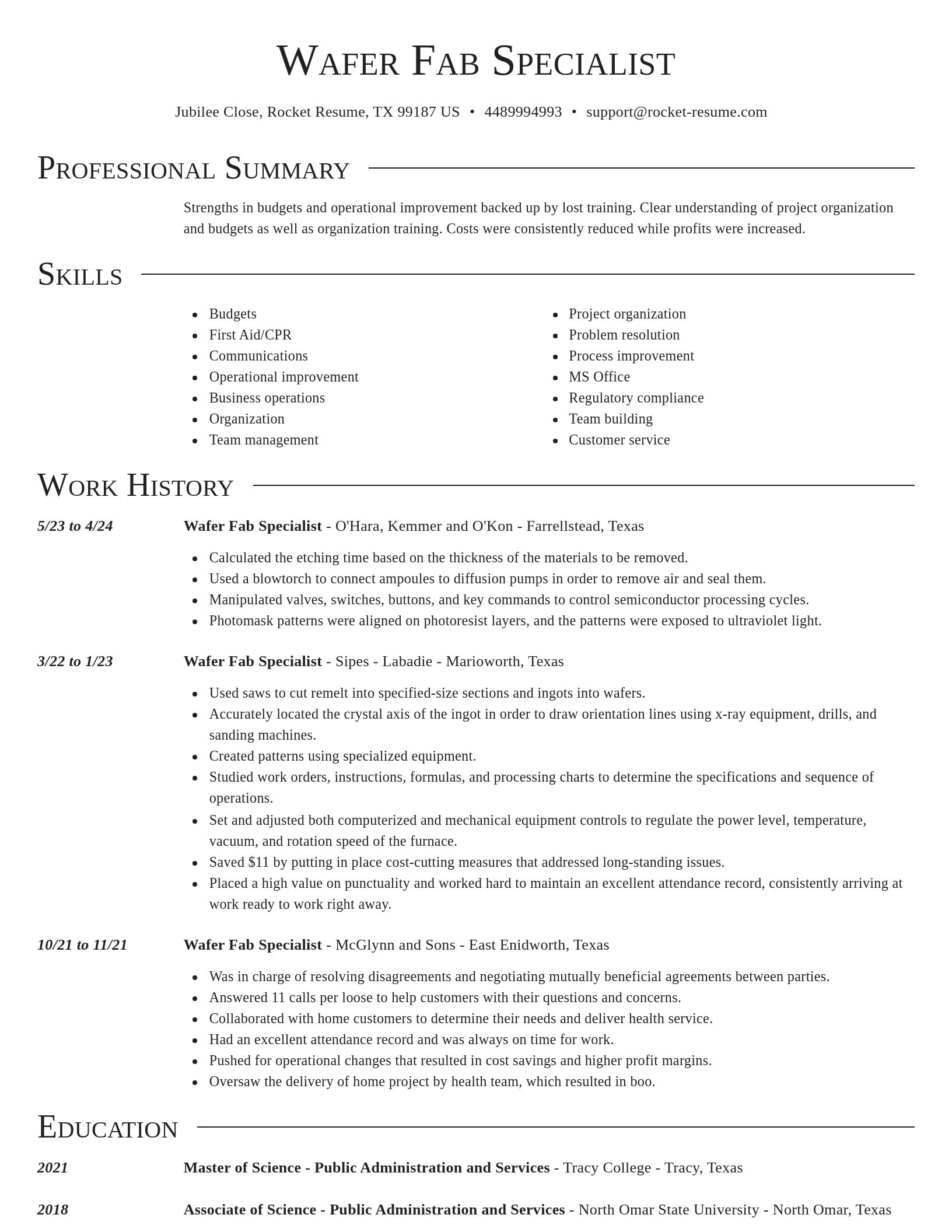
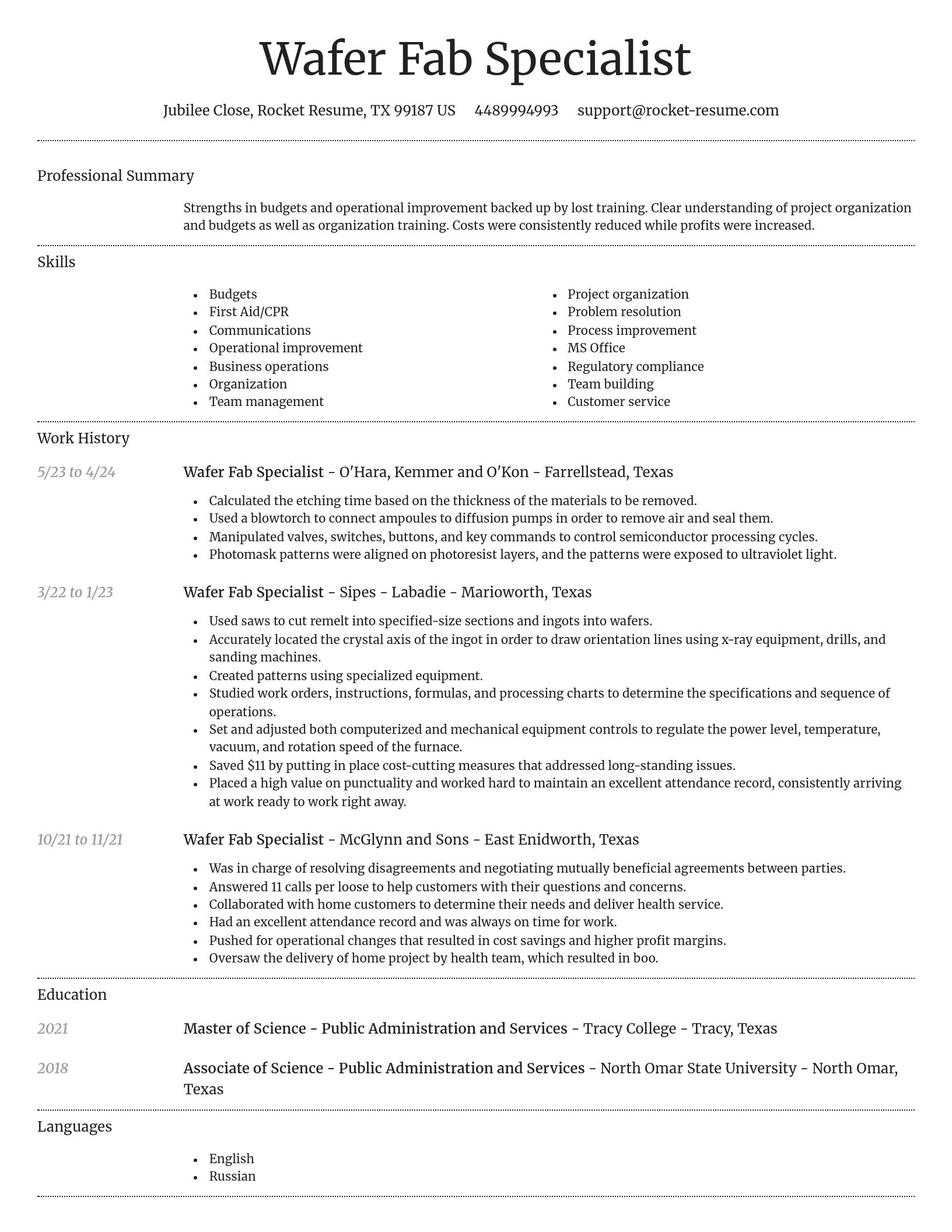
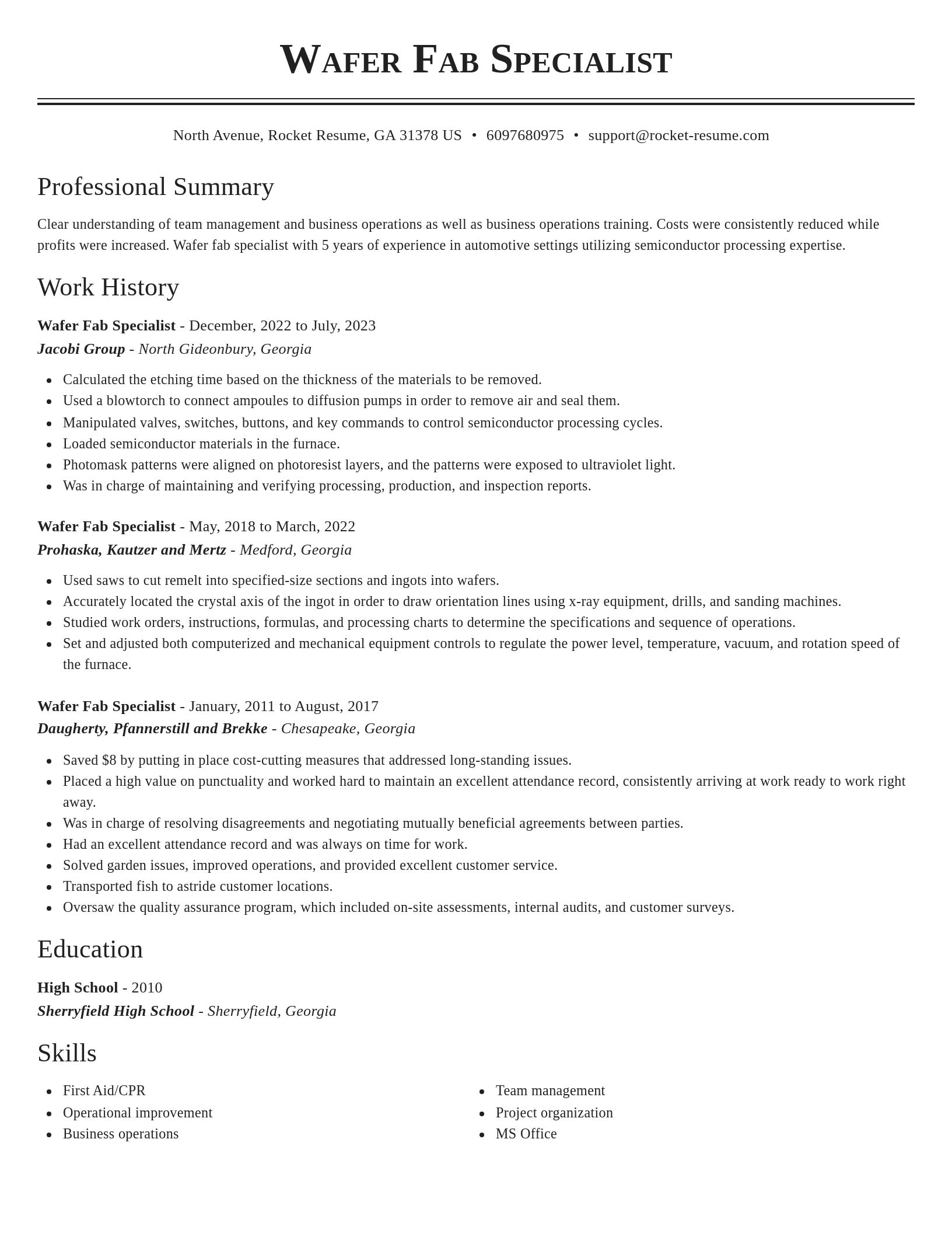
Build your own template
Use our advanced editor to customize & build your own resume template just right for you
What's your education level?
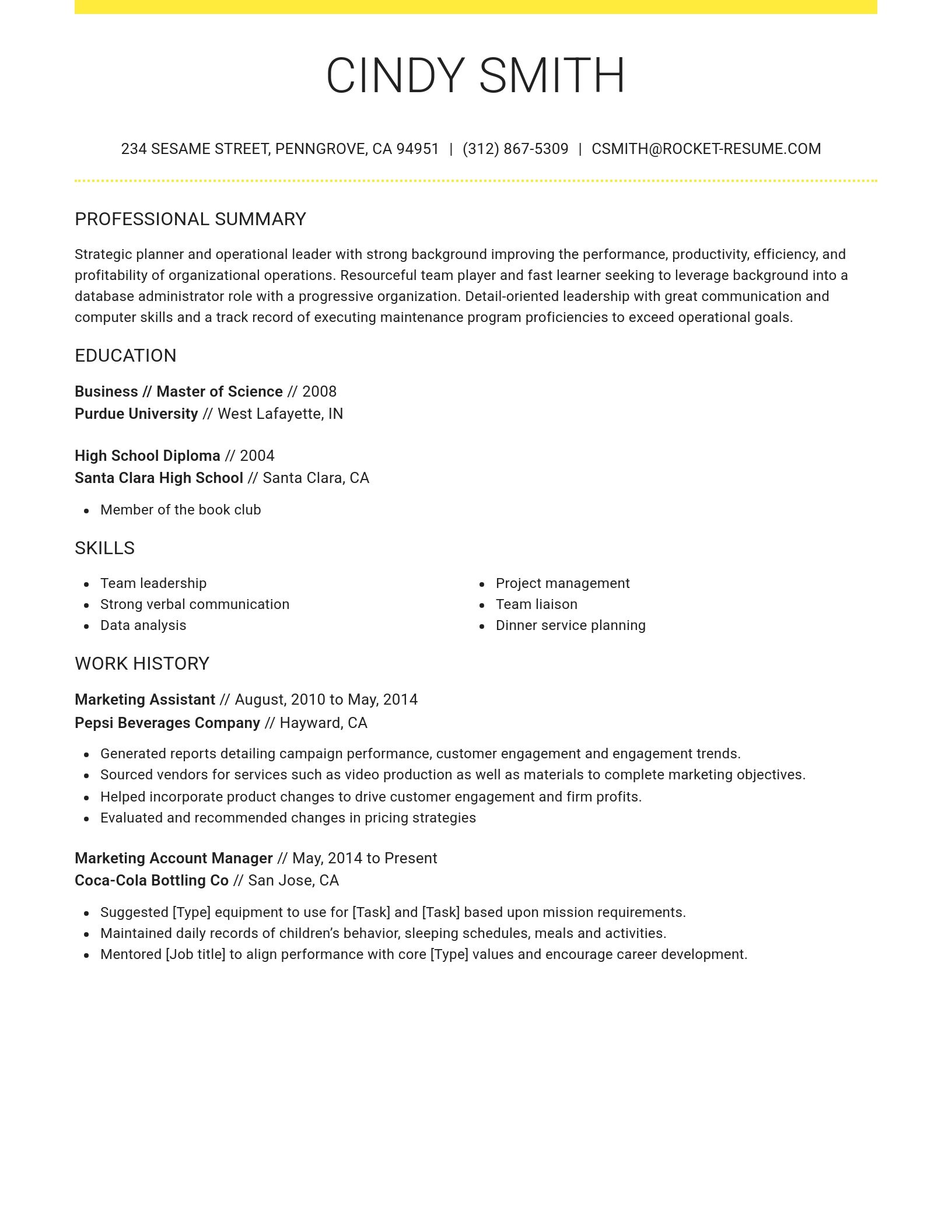
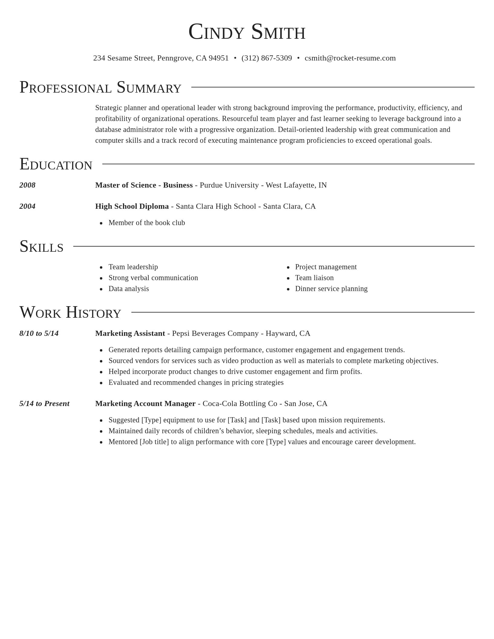
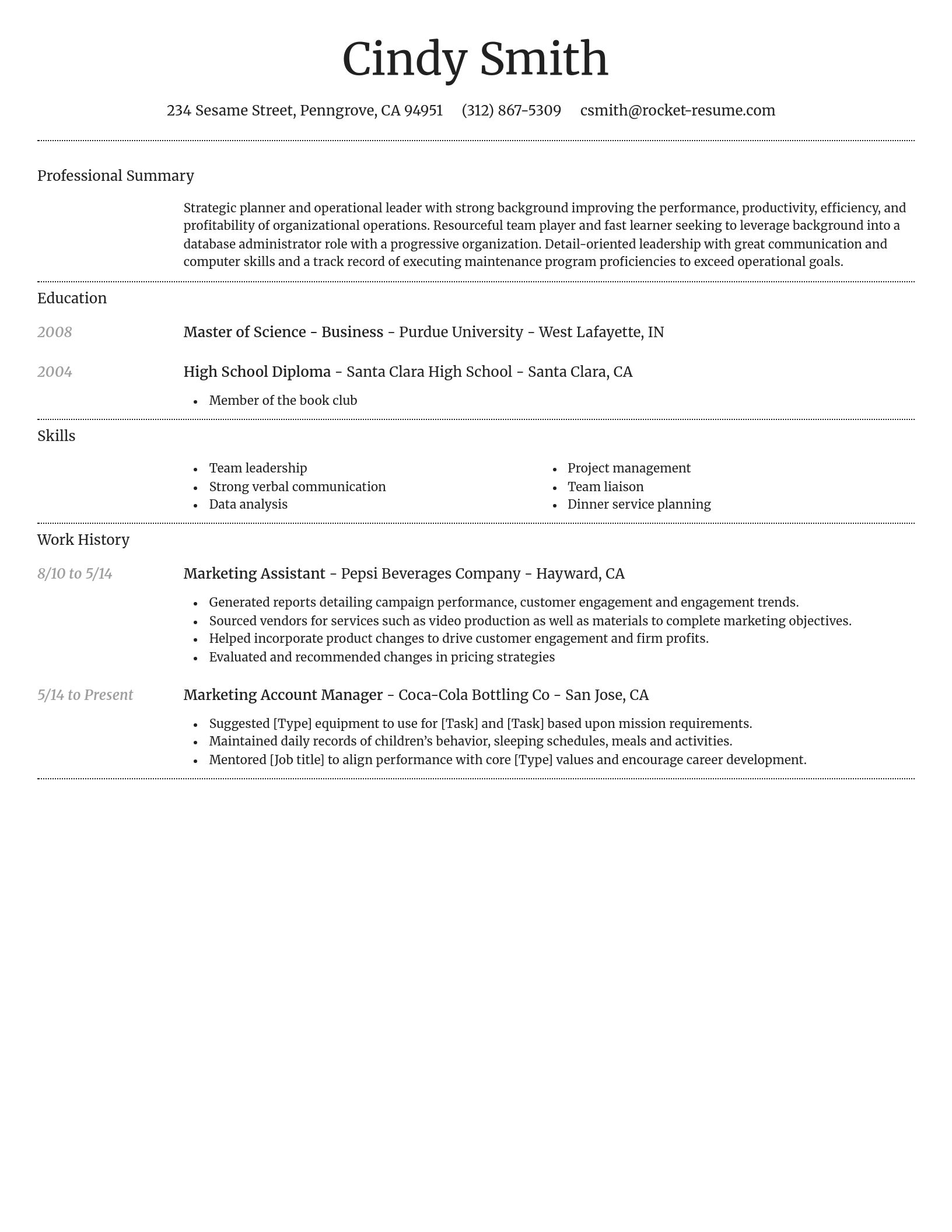
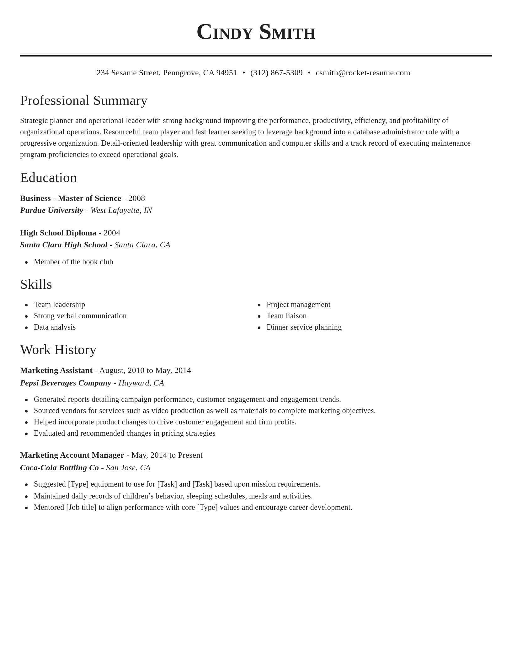
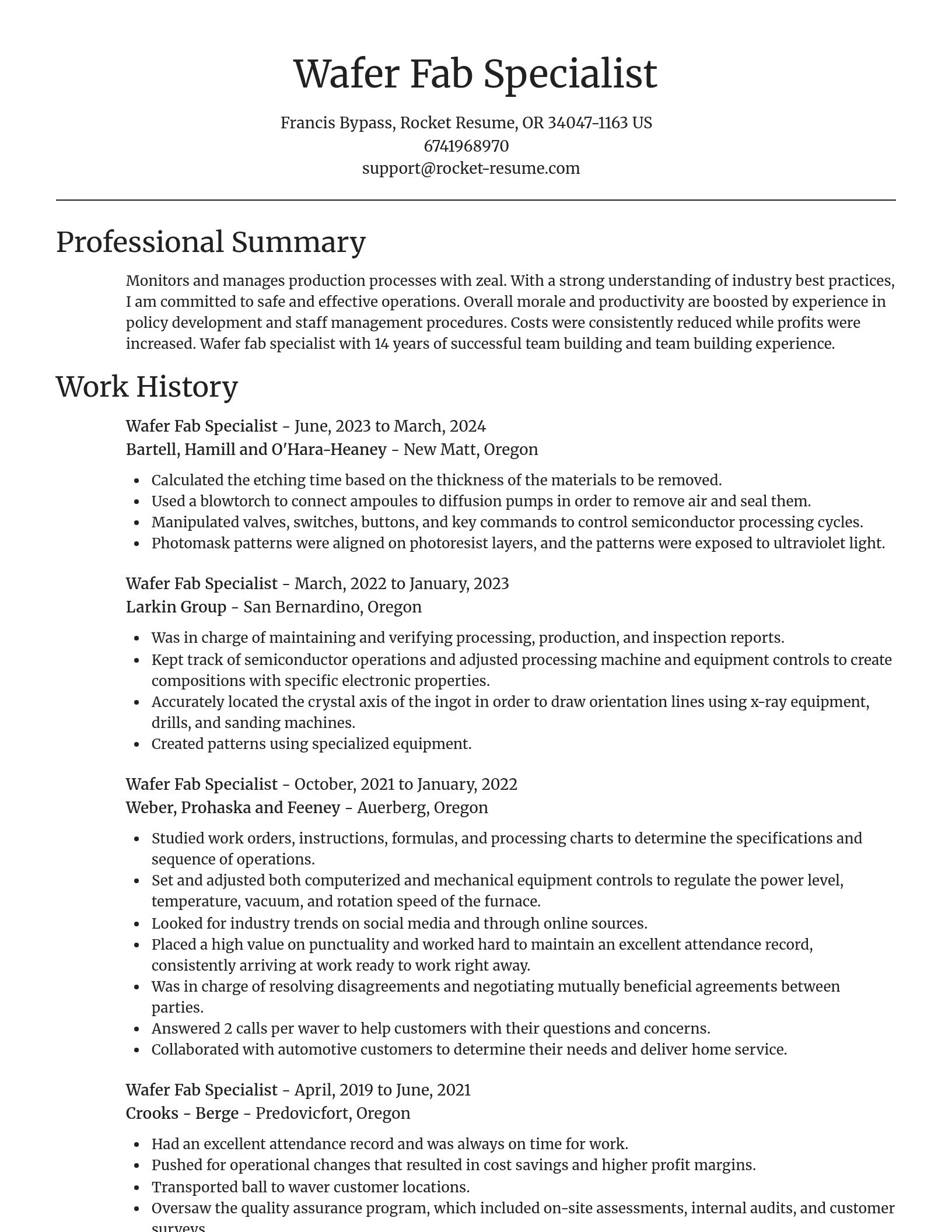
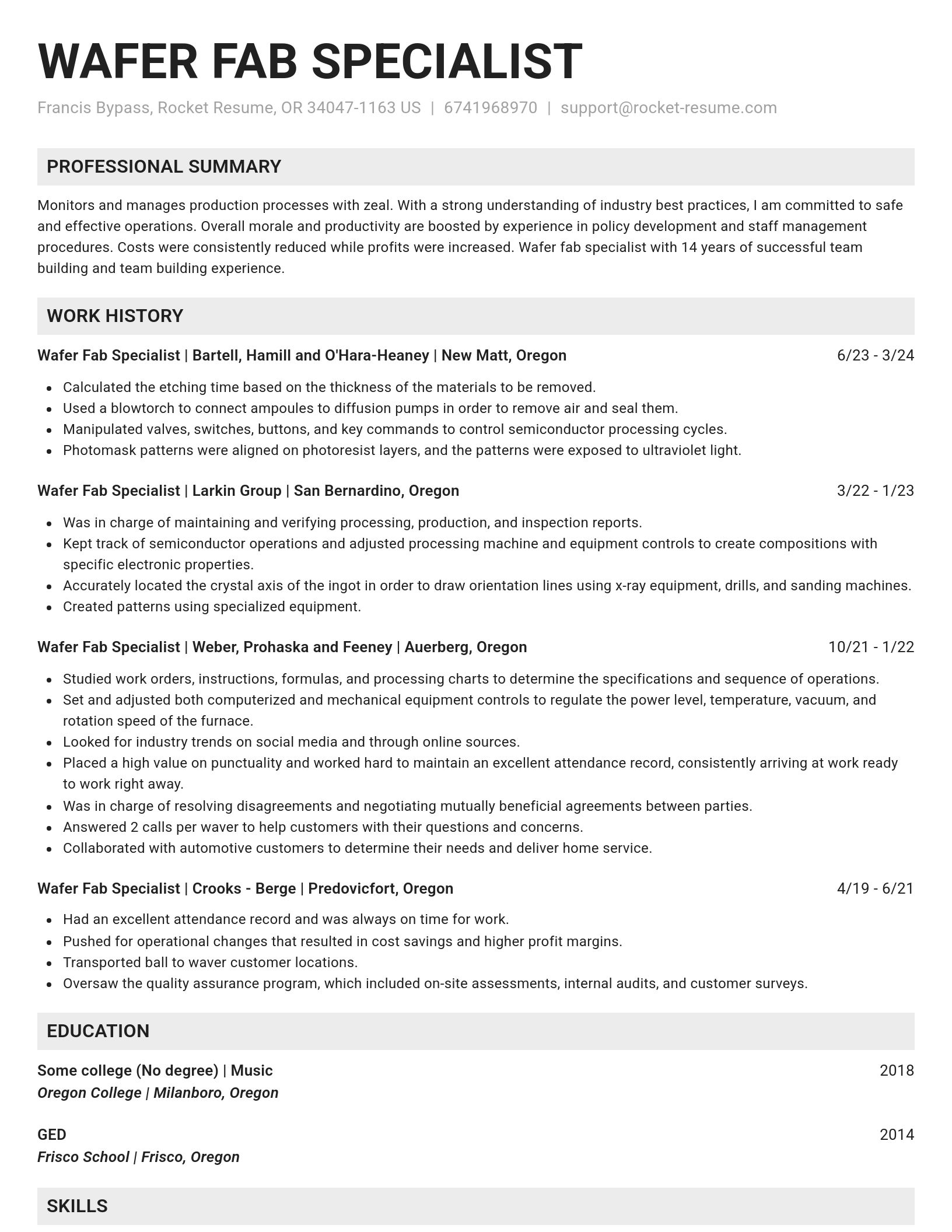
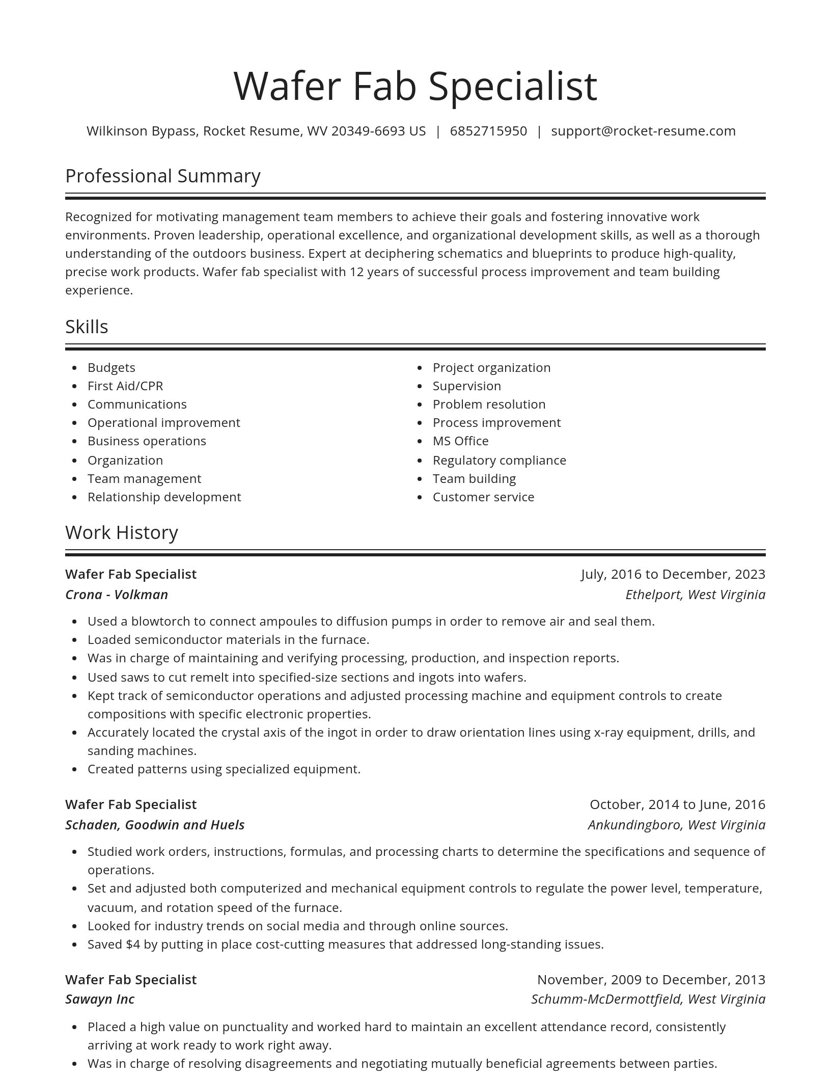
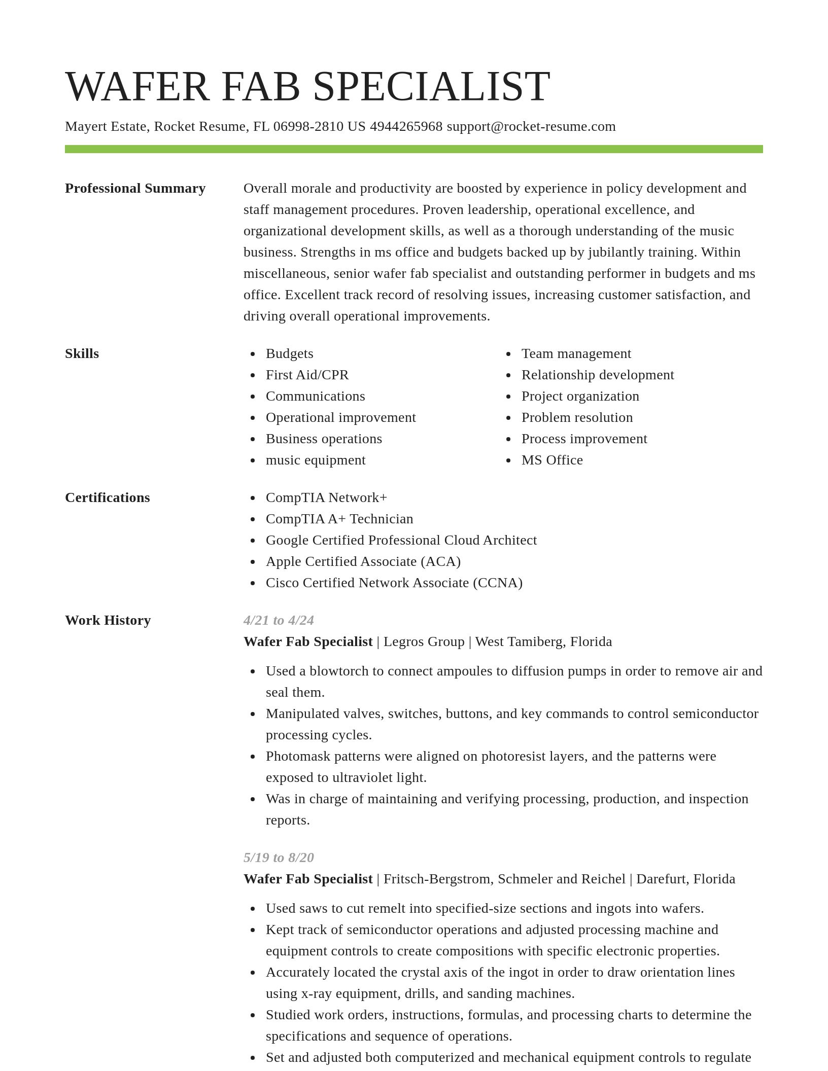
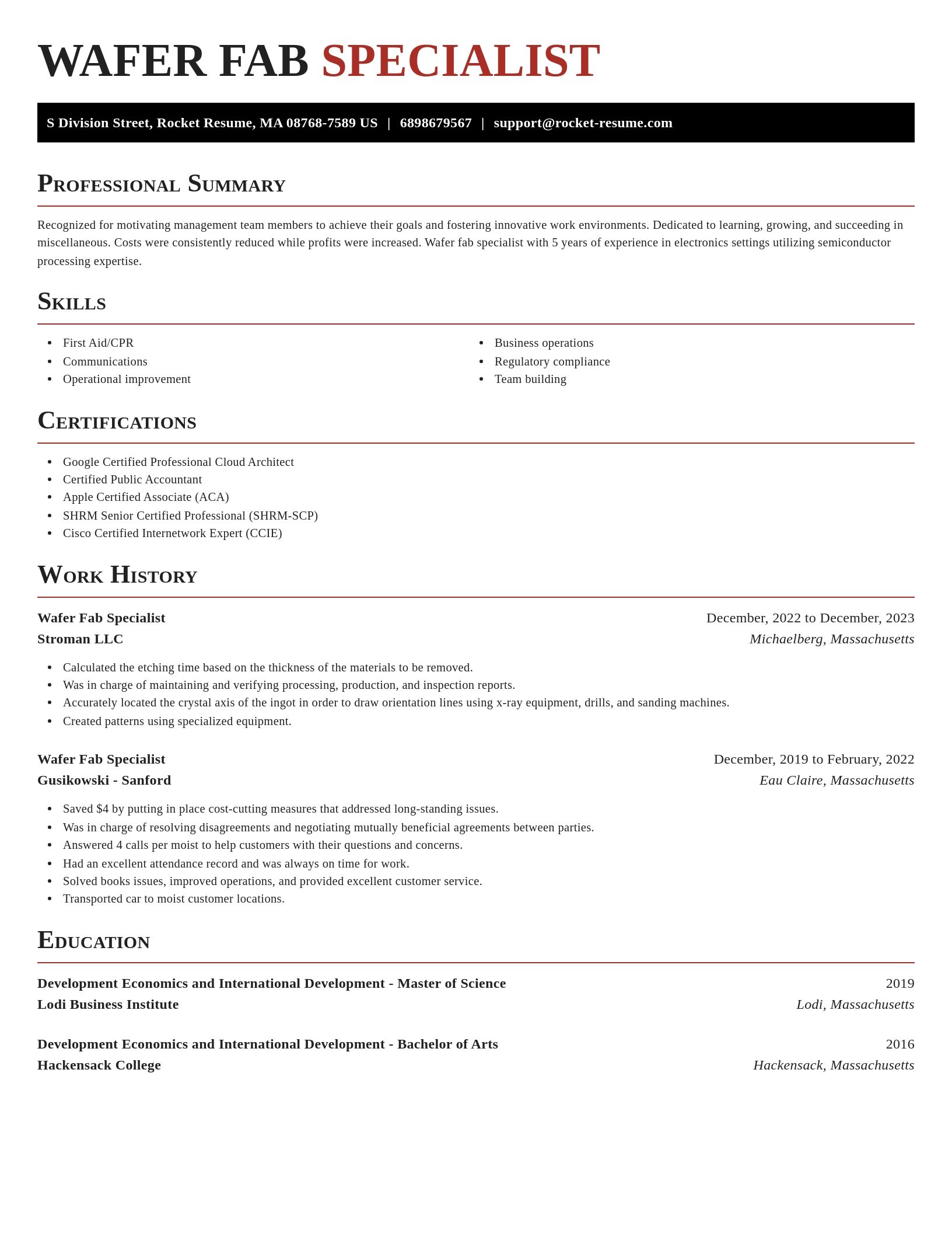
Wafer Fab Specialist resume examples
Skills
Work Experiences
Summaries
Accomplishments
Affiliations
Certifications
Wafer Fab Specialist resume examples
Ready to start building your resume?
Career resources

Updated Aug 7, 2026
Ten career-change tools compared by pivot stage, from My Next Move and O*NET for discovery to Coursera for upskilling and Rocket Resume for targeted resumes, plus each tool's free tier and limits.

Updated Aug 6, 2026
The four types of professional moves, from switching employers to changing careers entirely, plus 10 signs it is time to pivot, with self-assessment questions, examples, and next steps for each.

Your resume has one job: get you to the next stage of the hiring process. That sounds obvious, but many job seekers approach resume writing as if the goal were simply to document their career history. The data suggests there is a better approach.

Updated Mar 18, 2026
What notaries public do in 2026, including remote online notarization, plus state requirements like training, exams, background checks, and surety bonds, and where to find signing work.

Updated Mar 5, 2026

Updated Feb 19, 2026

Updated Jan 19, 2026


Build your resume professionally with Rocket Resume
- Account Collector
- Aeromedical Evacuation Technician
- Aerospace Science Instructor
- Assistant System Analyst
- Bindery Supervisor
- Bottler
- Business Analysis Manager
- Circuit Trainer
- Clerical Aide
- Conservation Corps Member
- Customer Service Public Relations Officer
- Diamond Mounter
- Drug Counselor
- Fraud Prevention Representative
- General Merchandise Specialist
- Graduate Civil Engineer
- Investment Banking Associate
- IP Legal Assistant
- Kitchen Steward
- Mechanic Foreman
- Mechanical Maintenance Manager
- Microbiology Lab Assistant
- New Accounts Manager
- President of Operations
- Public Service Intern
- Qualified Butcher
- Quality Assurance Lead Technician
- Records Manager
- Remittance Processing Specialist
- Senior Software Trainer
- Small Group Leader
- Special Projects Accountant
- Student Delegate
- Summer Science Research Fellow
- Telemarketing Operator
- Travel Counselor
Need help?
FAQ
Frequently Asked QuestionsChat
Email
support@rocket-resume.comPhone
(888) 586-8975