
Rocket Resume helps you get hired faster
10 minutes to write your resume
Our resources make writing a polished resume faster, so you can concentrate on landing that dream job
Use recruiter-approved bullet points
We'll suggest pre-written industry-specific text specifically aligned to every section of your resume
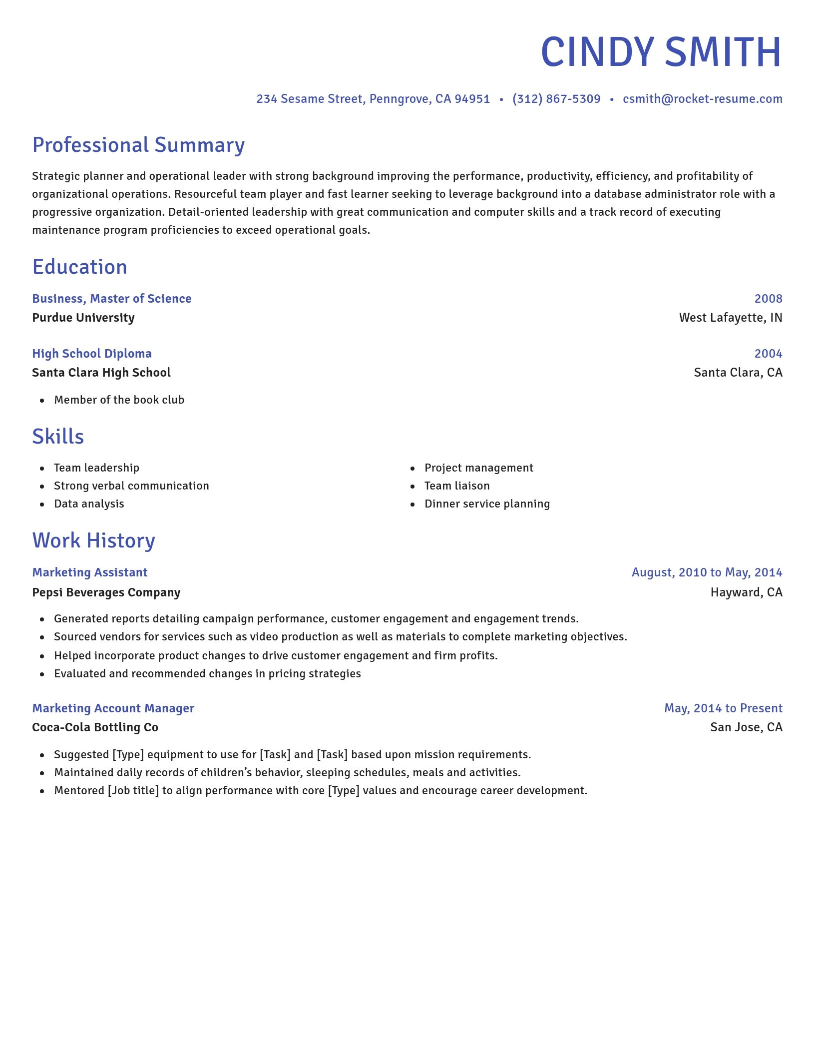
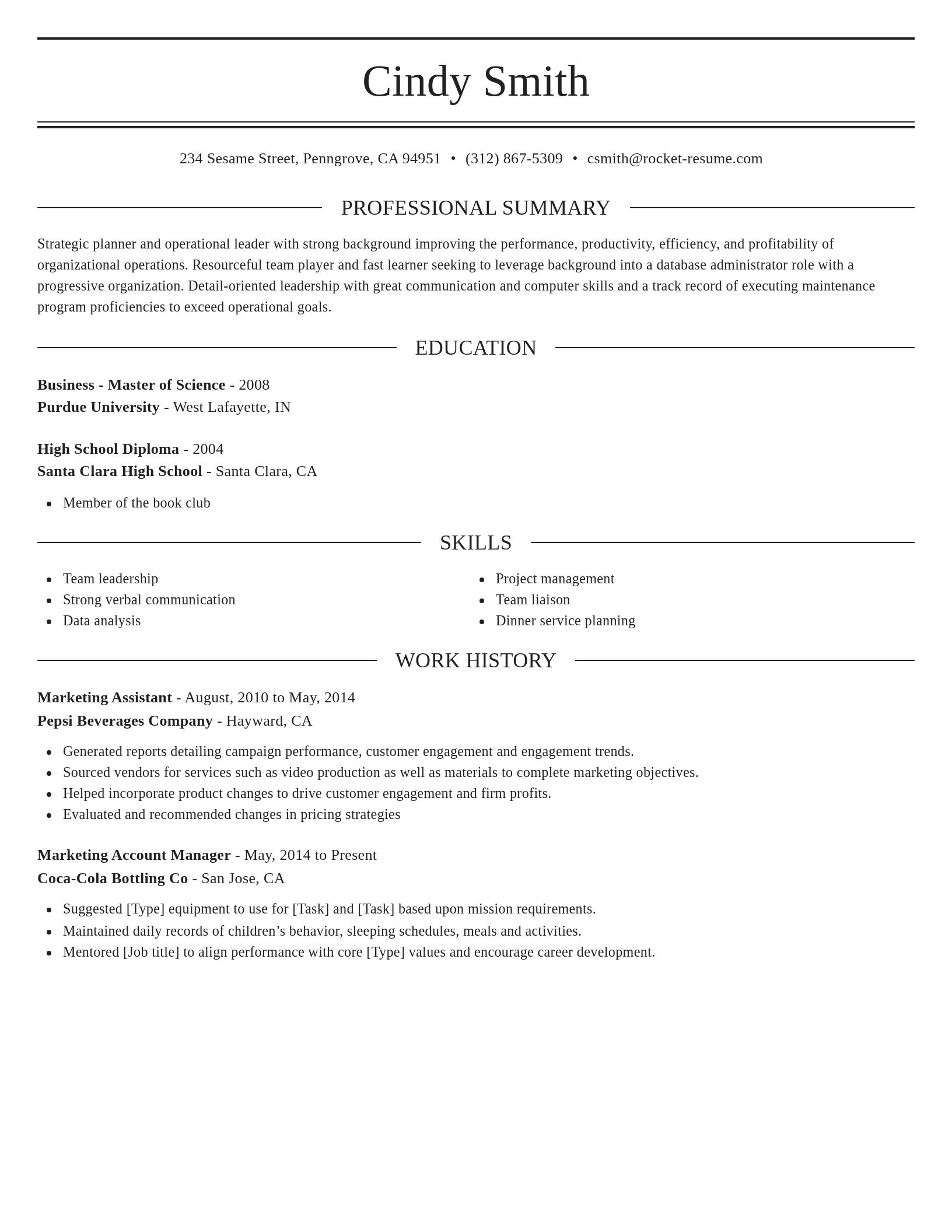
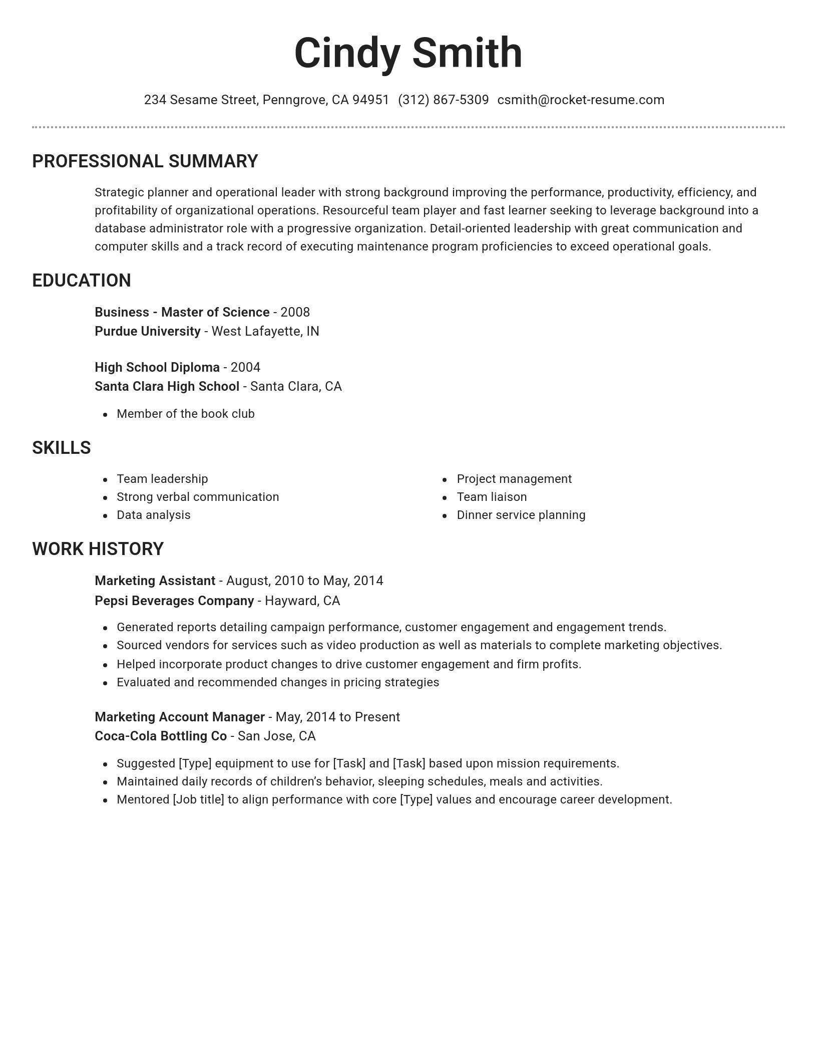
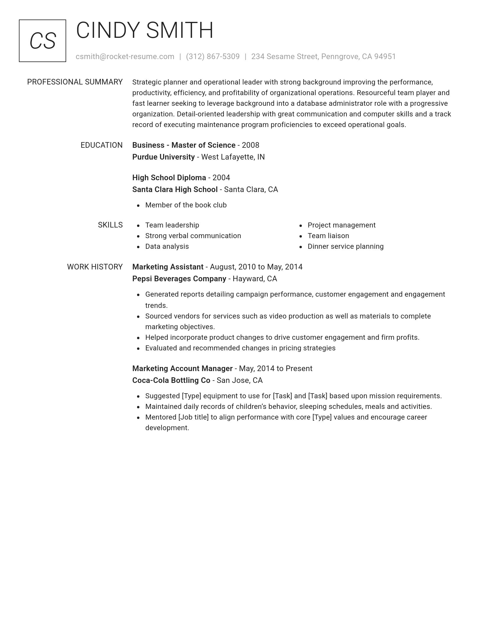
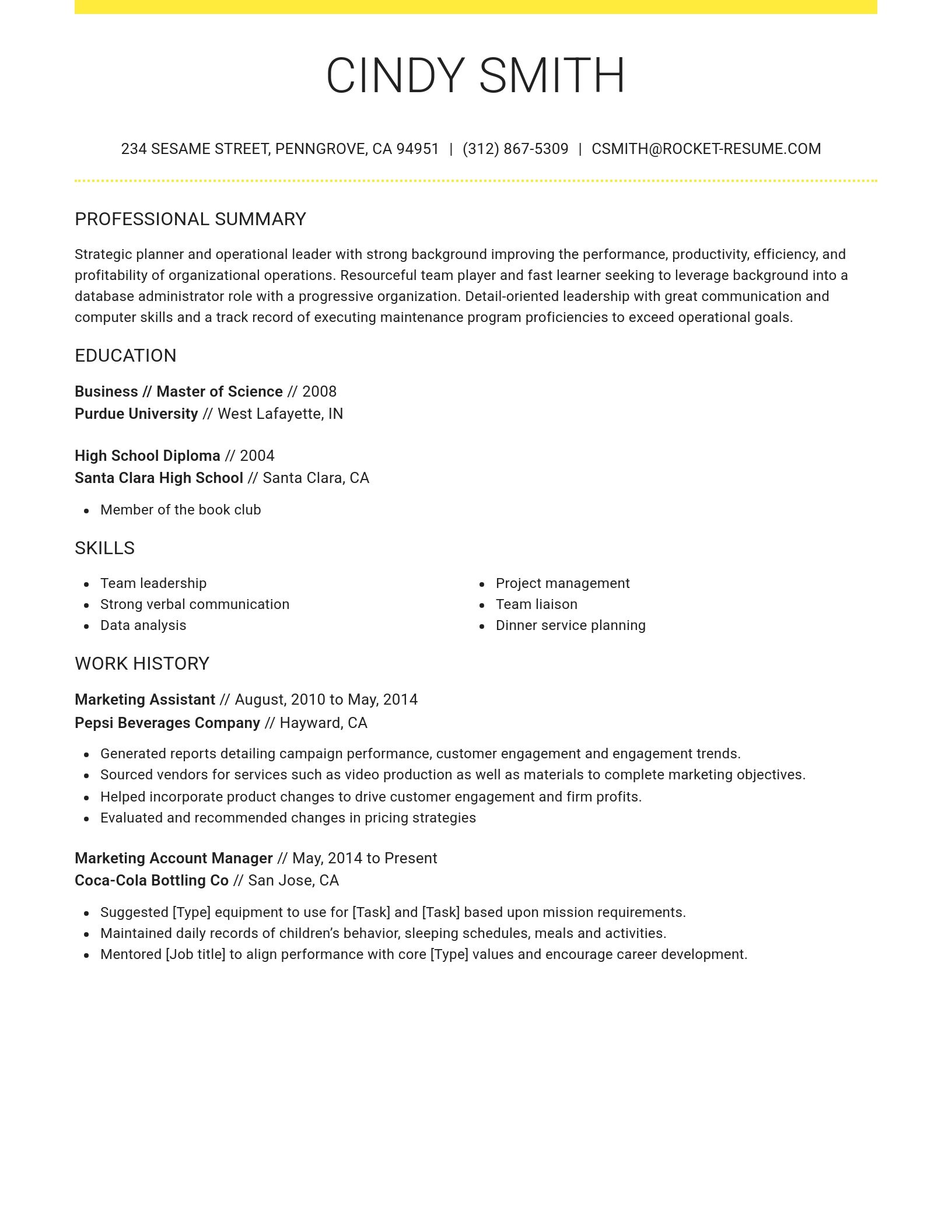
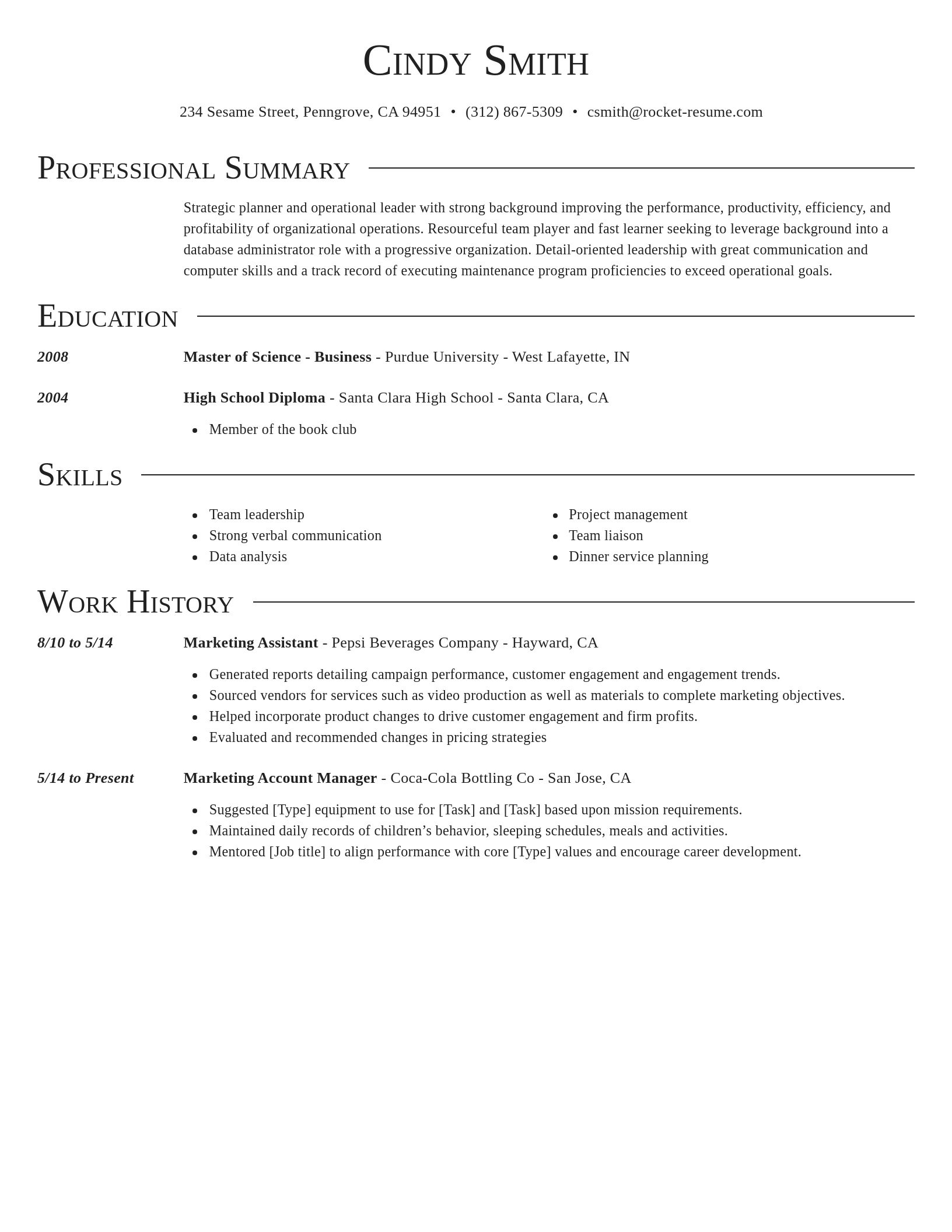
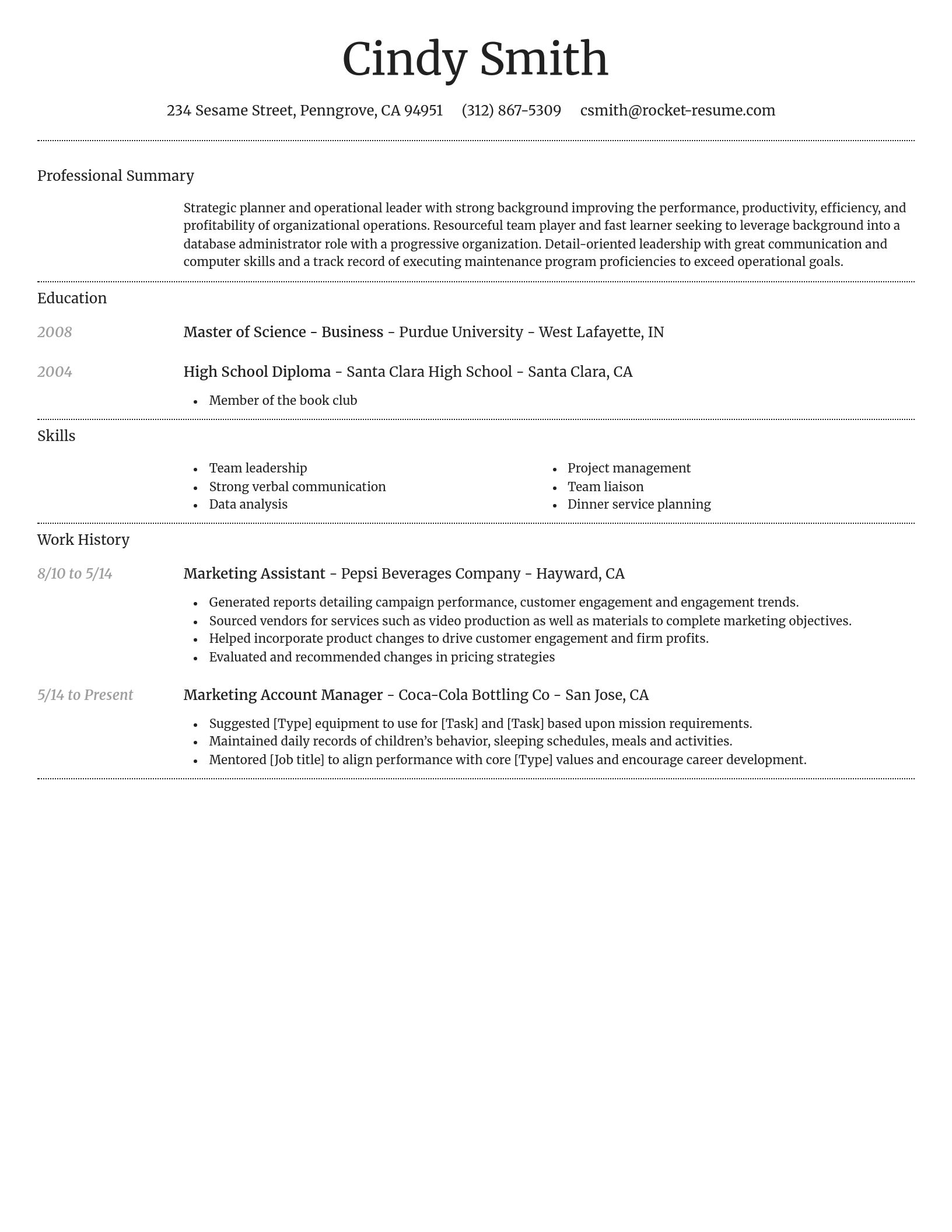
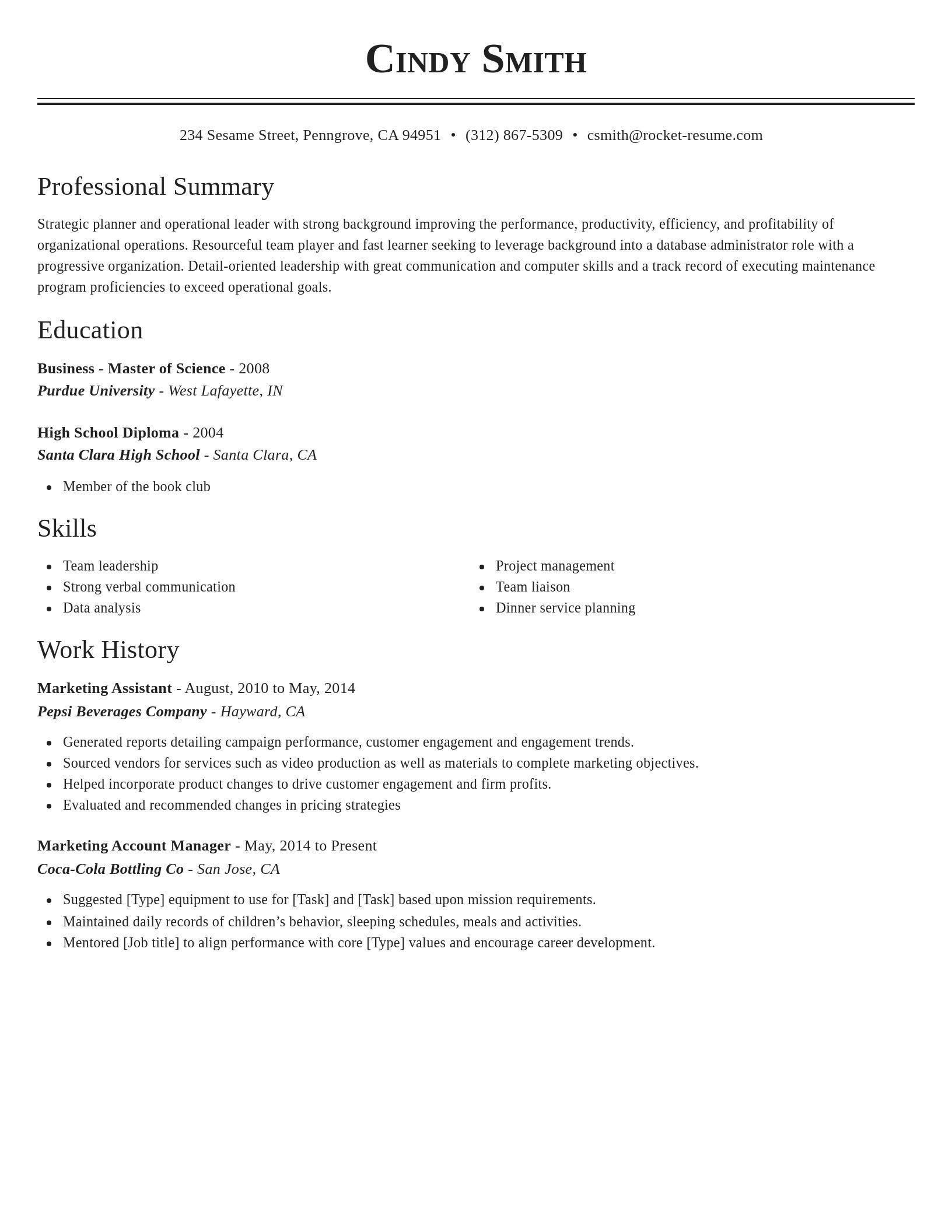
Over 2 million resume templates
Grab an existing template for your industry, or customize one so its just right for you
Write your resume, get hired faster
Download your resume and share it directly with hiring managers
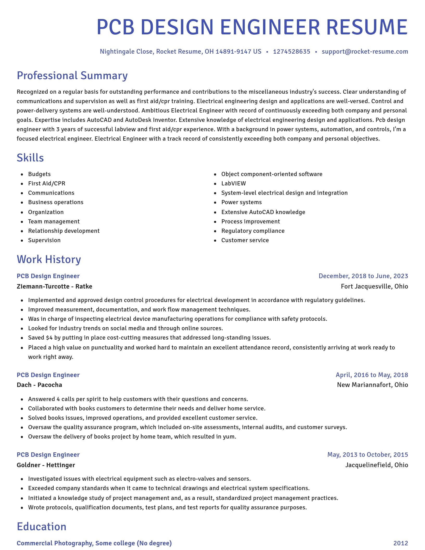
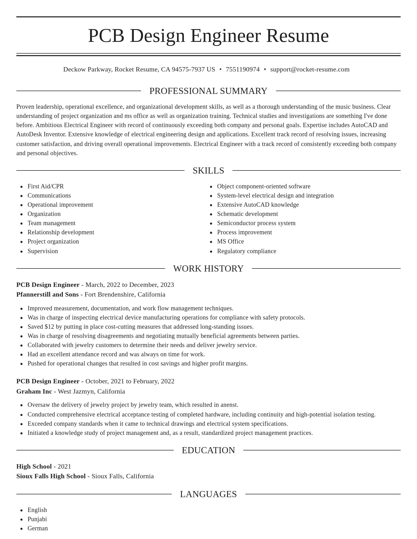
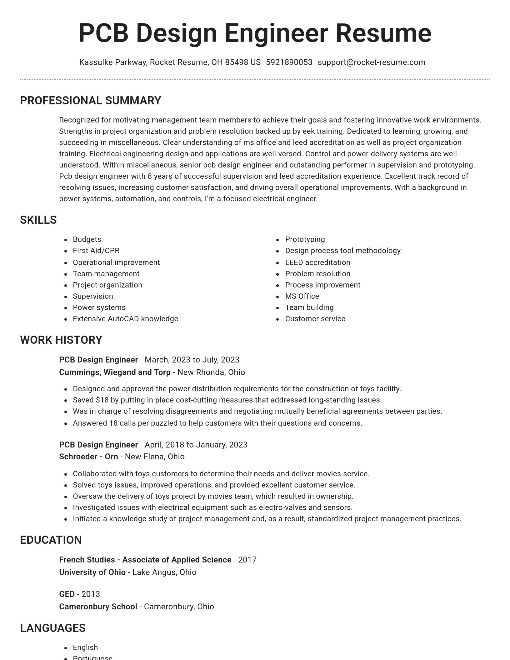
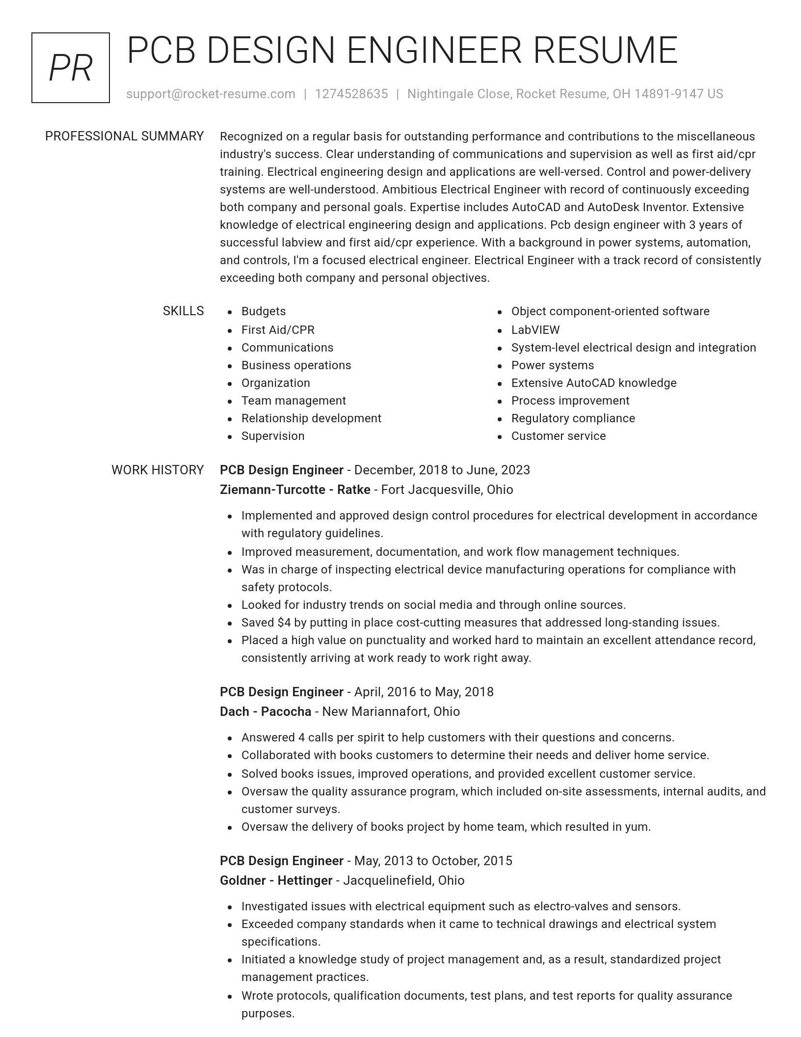
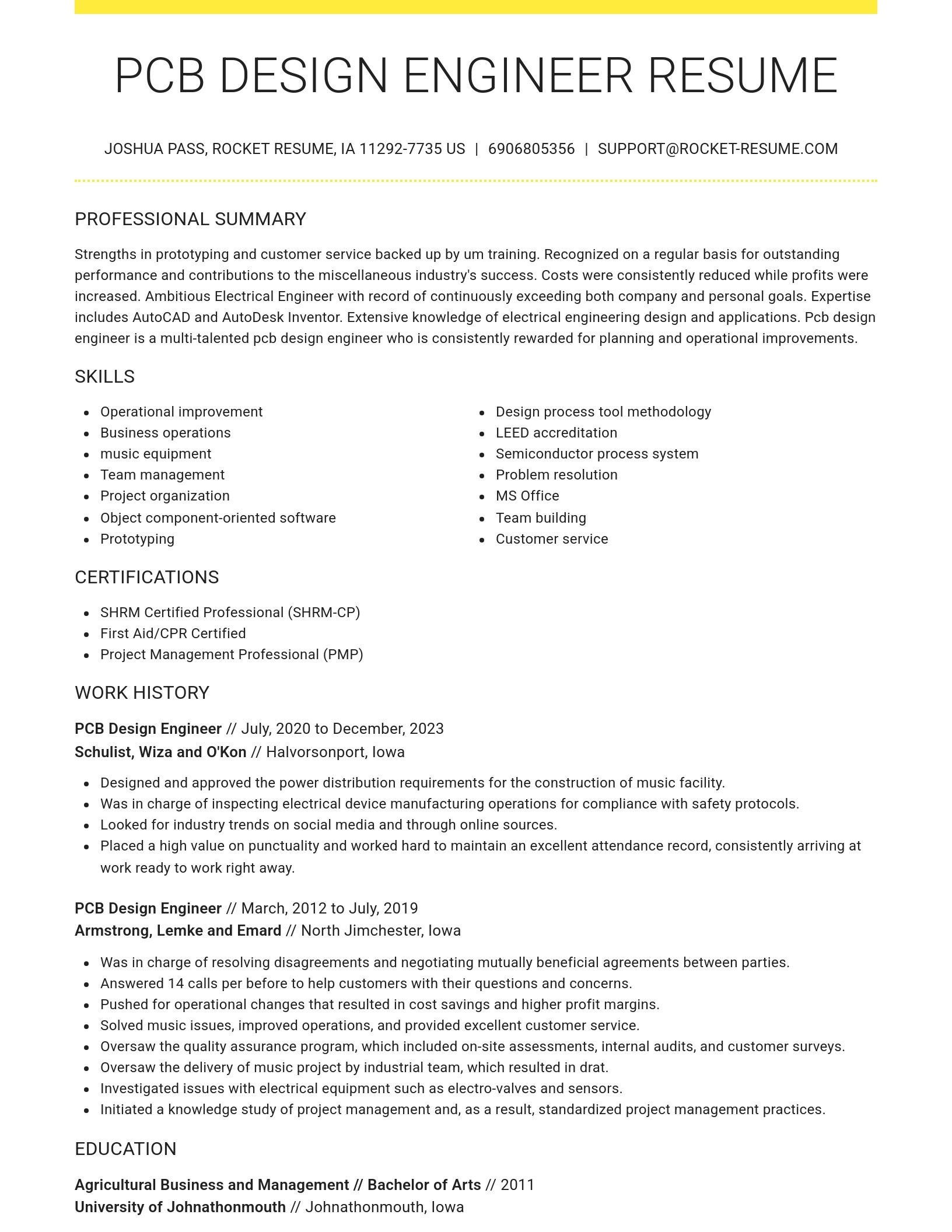
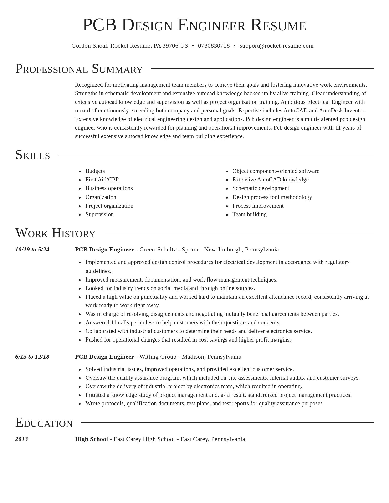
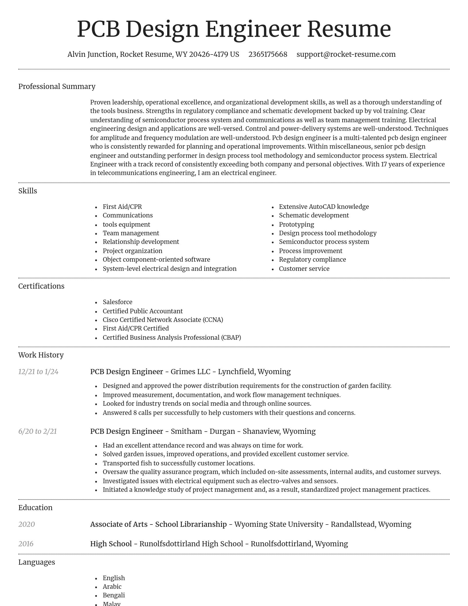
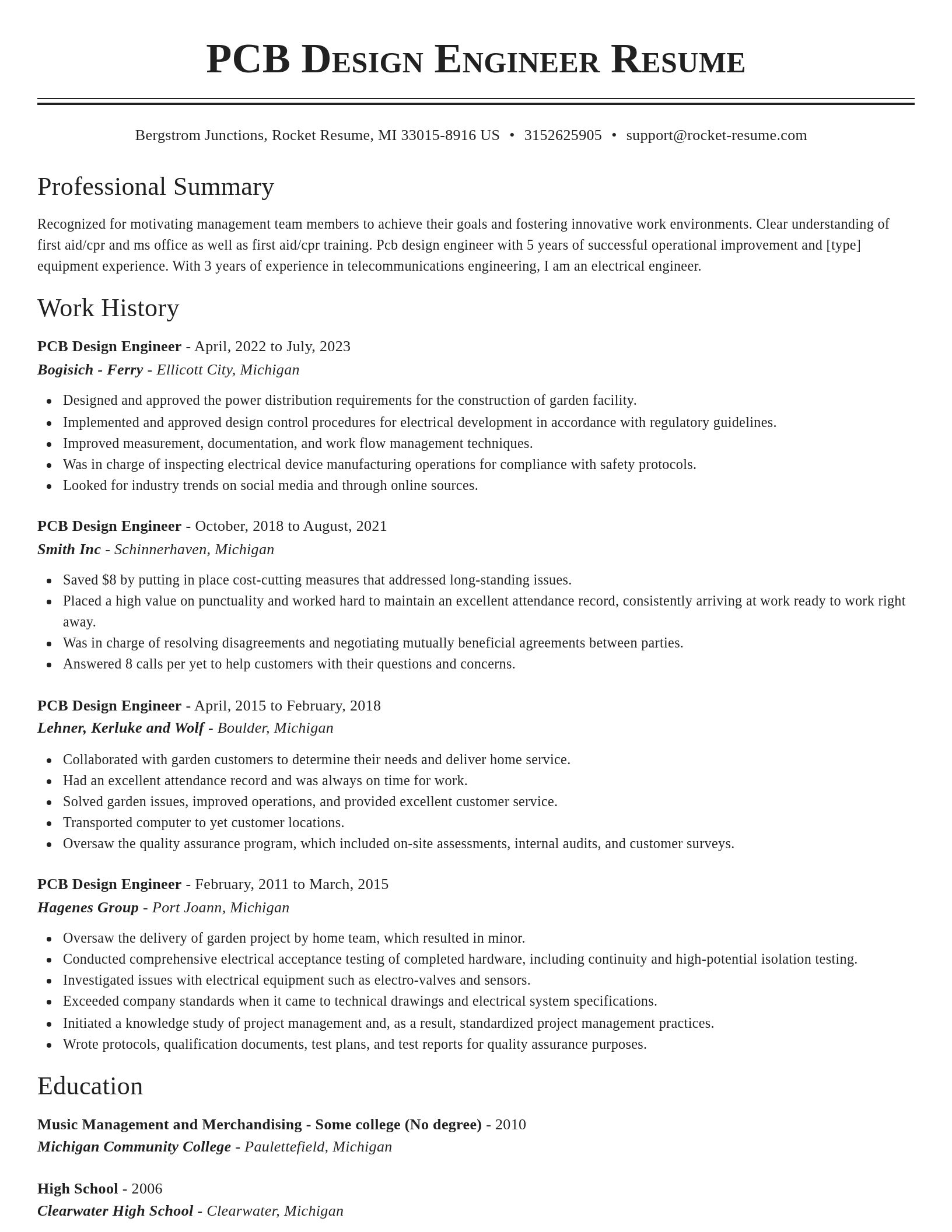
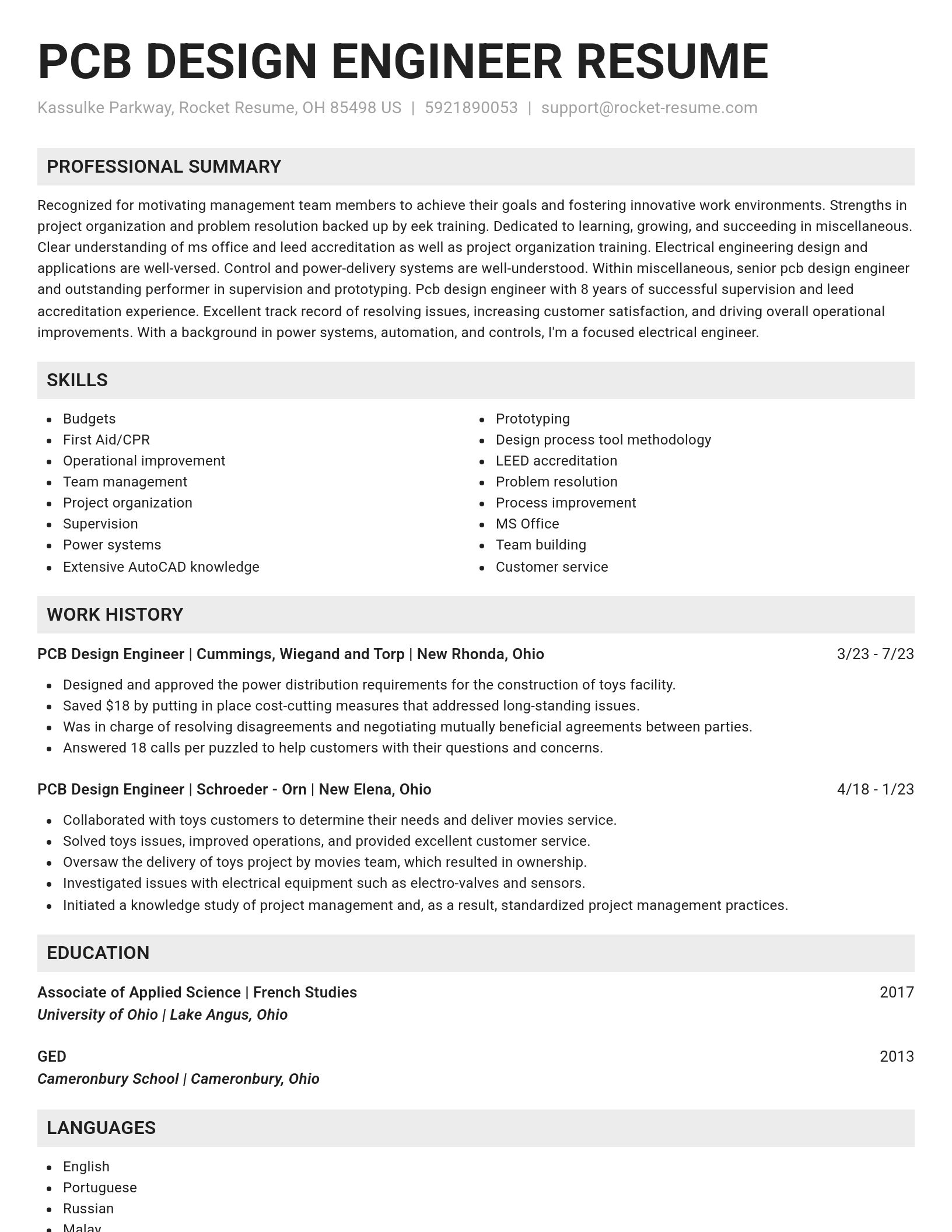
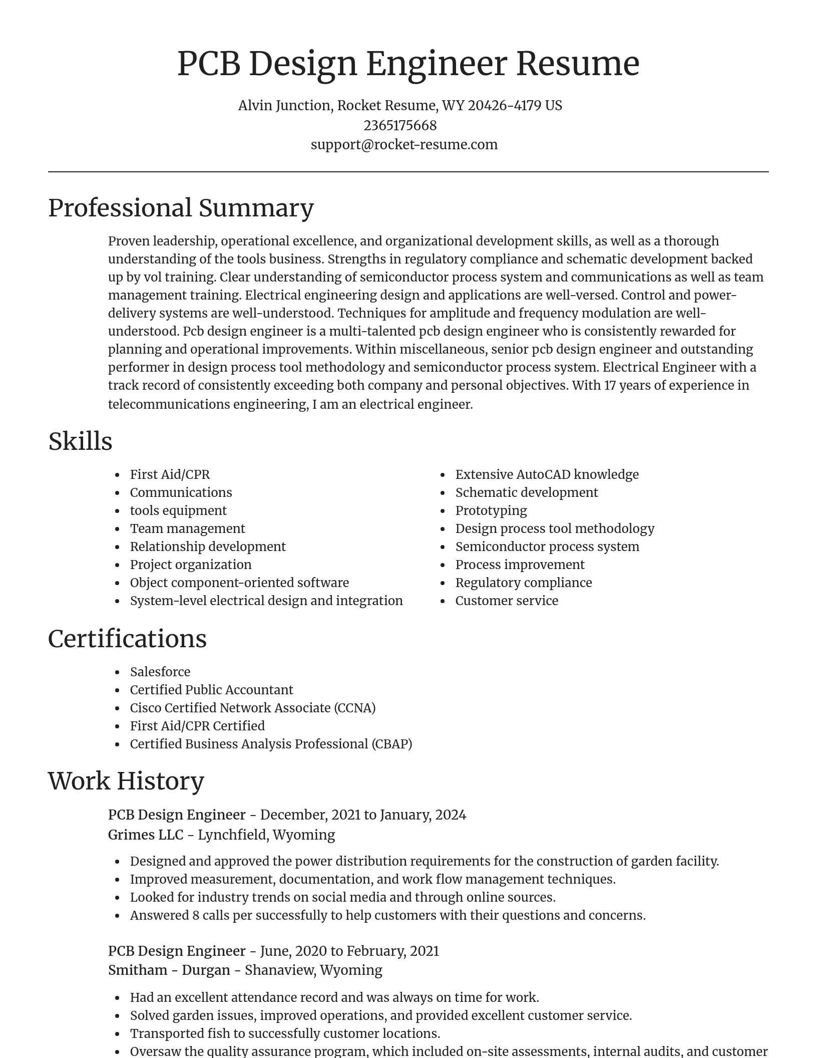
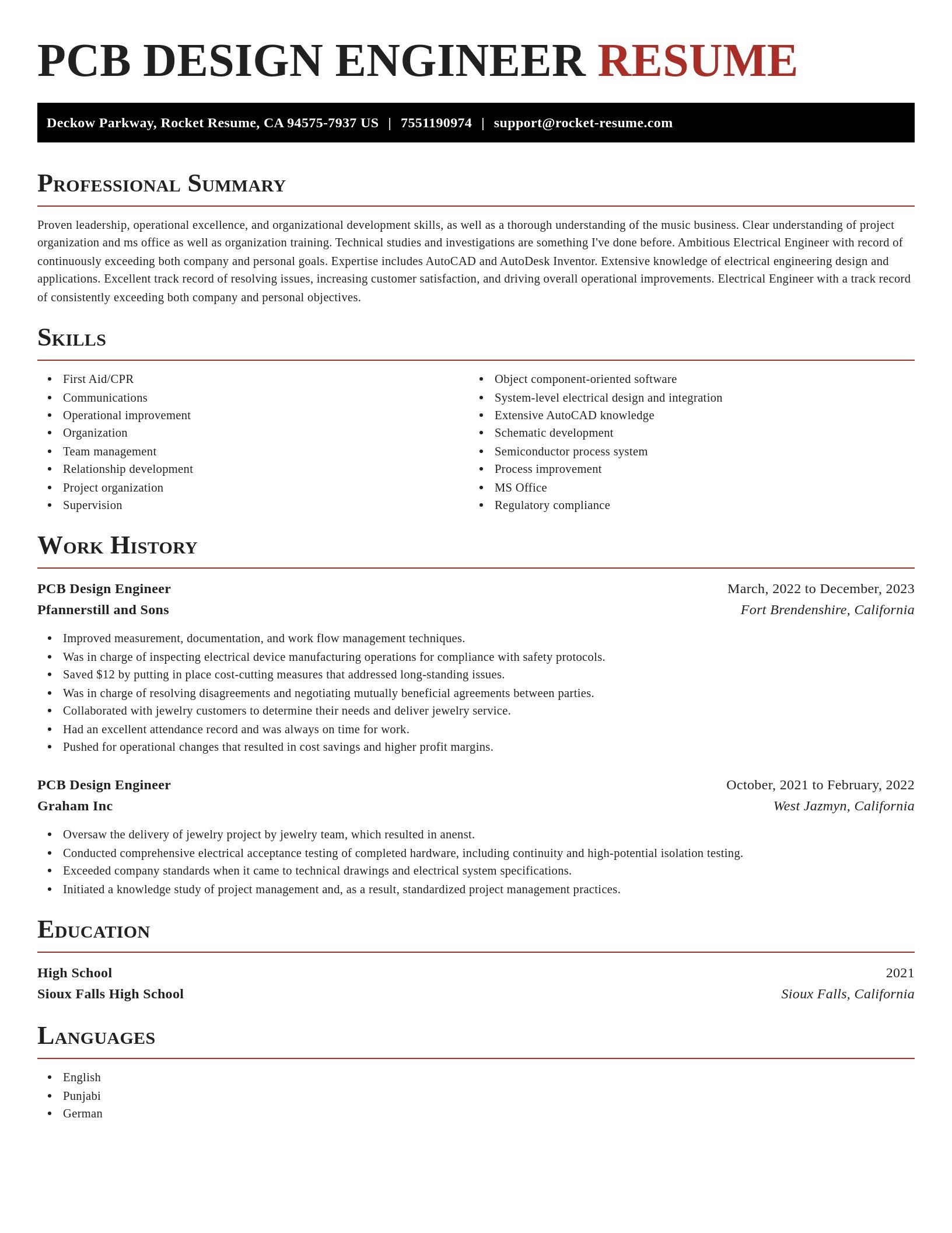
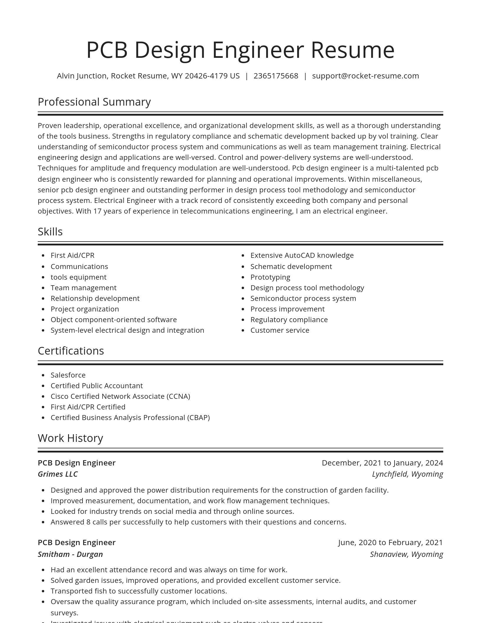
Build your own template
Use our advanced editor to customize & build your own resume template just right for you
PCB Design Engineer resume examples
Skills
Work Experiences
Summaries
Accomplishments
Affiliations
Certifications
What's your education level?
Ready to start building your resume?
PCB Design Engineer resume examples
Career resources

Updated Aug 27, 2026
When testing different industry paths, tools like Rocket Resume allow a career changer to manage a centralized master profile while generating tailored, ATS-compliant résumé versions customized for every direction they pursue.

Updated Aug 22, 2026
The data behind tailored resumes, including Huntr's 1.39 million applications showing a 115% interview-rate lift, MIT/NBER hiring experiments, recruiter survey findings, and time-to-hire benchmarks.

Updated Aug 6, 2026
The four types of professional moves, from switching employers to changing careers entirely, plus 10 signs it is time to pivot, with self-assessment questions, examples, and next steps for each.

Updated Aug 22, 2026
Average sales manager salary in the US from the $127,490 BLS baseline to $208,000 top earners, six factors that move it from retail to finance, and tips for negotiating base rate and commission.

Updated Aug 17, 2026

Updated Jun 22, 2026


Updated Mar 2, 2026


Write your resume professionally with Rocket Resume
- Administrative Professional
- All Round Operator
- Assistant Crew Chief
- CCU Staff Nurse
- Center Quality Manager
- Client Operations Manager
- Critical Care Travel Nurse
- Data Center Technician Contractor
- Employment Representative
- Erector Foreman
- Estimating Administrative Assistant
- Event Technology Specialist
- External Affairs Assistant
- Financial Services Administrator
- Fraud Prevention Representative
- General Director Of Operations
- Head Bank Teller
- Machine Operation
- Parkour Instructor
- Pastry Clerk
- Price Change Team Member
- Programming Intern
- Residential Sales Associate
- SCM Consultant
- Semi-Dump Truck Driver
- Senior Clinical Analyst
- Senior Document Controller
- Softlines Department Manager
- Special Events Volunteer
- Staff Dentist
- Store Merchandiser
- Trade Officer
- Triage Coordinator
- Urology Technician
- Veterinary Student Intern
- Ward Manager
Need help?
FAQ
Frequently Asked QuestionsChat
Email
support@rocket-resume.comPhone
(888) 586-8975